Hole selective MoO<x>/SiO<x>(Mo)/n-Si heterojunction, solar cell device and fabrication method of solar cell device

A solar cell and heterojunction technology, applied in electrical components, semiconductor devices, circuits, etc., can solve the problems of reduced recombination, narrow process window, expensive equipment, etc.

Active Publication Date: 2018-11-23
SHANGHAI UNIV
View PDF8 Cites 2 Cited by
  • Summary
  • Abstract
  • Description
  • Claims
  • Application Information

AI Technical Summary

Problems solved by technology

In 2014, C. Battaglia et al. used vacuum evaporation technology to deposit 15nm thick MoO on n-Si substrates x thin film, prepared for the first time with MoO x A silicon-based heterojunction photovoltaic device with a hole-selective contact layer obtained a photoelectric conversion efficiency (η) of 14.3%, due to MoO x / n-Si interface without additional passivation treatment, the open circuit voltage (V oc ) is only 580mV; subsequently, C.Battaglia et al. in MoO x Intrinsic hydrogenated amorphous silicon (a-Si:H(i)) is introduced into the / n-Si interface region, which greatly reduces the MoO x / n-Si interface recombination, so that V oc and η reach 711mV and 18.8%, respectively, but the fill factor (FF) is only 67.2% (at this time, the electrode annealing temperature is 200°C, N 2 atmosphere)
Considering that a-Si:H(i) has problems such as parasitic absorption and narrow process window, and the deposition of a-Si:H(i) layer requires expensive equipment

Method used


Image

  • Hole selective MoO&lt;x&gt;/SiO&lt;x&gt;(Mo)/n-Si heterojunction, solar cell device and fabrication method of solar cell device
  • Hole selective MoO&lt;x&gt;/SiO&lt;x&gt;(Mo)/n-Si heterojunction, solar cell device and fabrication method of solar cell device
  • Hole selective MoO&lt;x&gt;/SiO&lt;x&gt;(Mo)/n-Si heterojunction, solar cell device and fabrication method of solar cell device

Examples


Embodiment 1

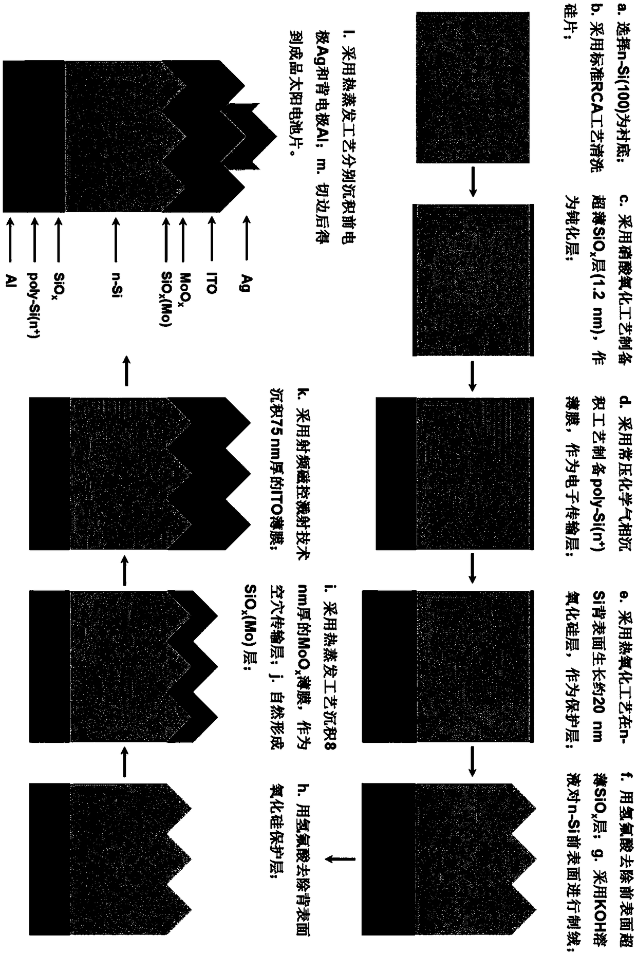
[0046] In this example, see Figure 1 to Figure 7 , a hole-selective MoO x / SiO x (Mo) / n-Si heterojunction using MoO x / SiO x (Mo) stacked composite thin film material is matched with the n-Si material layer to form a hole-selective passivation contact heterojunction to obtain MoO x / SiO x (Mo) / n-Si heterojunction; wherein, the MoO x / SiO x Ultrathin SiO in (Mo)Laminated Composite Thin Film Materials x (Mo) film is in MoO x Ultrathin SiO containing Mo element formed between film and n-Si substrate x Thin films, MoO during thermal evaporation 3 Molecular groups, Mo, and O atoms move to the front surface of the single crystal silicon wafer, and react with the shallow silicon atoms of the single crystal silicon wafer to form ultra-thin SiO x (Mo) thin film layer, ultra-thin SiO x (Mo) The mass percentage of Mo in the thin film layer is 30%.

[0047] In this example, in MoO x / SiO x (Mo) / n-Si laminated composite film, MoO x The thickness of the film layer is 8nm and...

Embodiment 2

[0074] This embodiment is basically the same as Embodiment 1, especially in that:

[0075] In this example, a hole-selective MoO x / SiO x (Mo) / n-Si heterojunction using MoO x / SiO x (Mo) stacked composite thin film material is matched with the n-Si material layer to form a hole-selective passivation contact heterojunction to obtain MoO x / SiO x (Mo) / n-Si heterojunction; wherein, the MoO x / SiO x Ultrathin SiO in (Mo)Laminated Composite Thin Film Materials x (Mo) film is in MoO x Ultrathin SiO containing Mo element formed between film and n-Si substrate x Thin films, MoO during thermal evaporation 3 Molecular groups, Mo, and O atoms move to the front surface of the single crystal silicon wafer, and react with the shallow silicon atoms of the single crystal silicon wafer to form ultra-thin SiO x (Mo) thin film layer, ultra-thin SiO x (Mo) The mass percentage of Mo in the thin film layer is 30%.

[0076] In this example, in MoO x / SiO x (Mo) / n-Si laminated composite...

Embodiment 3

[0098] This embodiment is basically the same as the previous embodiment, and the special features are:

[0099] In this example, a hole-selective MoO x / SiO x (Mo) / n-Si heterojunction using MoO x / SiO x (Mo) stacked composite thin film material is matched with the n-Si material layer to form a hole-selective passivation contact heterojunction to obtain MoO x / SiO x (Mo) / n-Si heterojunction; wherein, the MoO x / SiO x Ultrathin SiO in (Mo)Laminated Composite Thin Film Materials x (Mo) film is in MoO x Ultrathin SiO containing Mo element formed between film and n-Si substrate x Thin films, MoO during thermal evaporation 3 Molecular groups, Mo, and O atoms move to the front surface of the single crystal silicon wafer, and react with the shallow silicon atoms of the single crystal silicon wafer to form ultra-thin SiO x (Mo) thin film layer, ultra-thin SiO x (Mo) The mass percentage of Mo in the thin film layer is 30%.

[0100] In this example, in MoO x / SiO x (Mo) / n-S...


PUM


Abstract

The invention discloses a hole selective MoO<x>/SiO<x>(Mo)/n-Si heterojunction, a solar cell device and a fabrication method of the solar cell device. The fabrication method comprises the steps of depositing a MoO<x> thin film by taking a single-crystal silicon wafer as a substrate, and enabling MoO3 molecular groups in vapor steam, Mo, O atoms and silicon atoms in a shallow layer of the single-crystal silicon wafer to generate solid-phase reaction to form an ultrathin SiO<x>(Mo) layer by hot evaporation; and forming a functional layer structure body of an interface composite solar cell device, and fabricating an IOT thin film and an electrode to obtain a solar cell piece. The MoO<x>/SiO<x>(Mo)/n-Si heterojunction solar cell is fabricated by combining a crystal silicon surface cleaning process, a MnO<x> thin film deposition process by hot evaporation, a low-energy vapor steam solid-phase reaction method, a ITO thin film deposition process by radio-frequency magnetron sputtering, a nitric acid oxidization process, a normal-pressure chemical vapor deposition thin film process and a hot evaporation metal electrode process, and has relatively good stability and relatively high photoelectric conversion efficiency.

Description

technical field [0001] The invention relates to a solar cell device and a preparation method thereof, in particular to a solar cell device with MoO x / n-Si structure heterojunction photovoltaic device and its preparation method, which are applied to the preparation technology of high-efficiency crystalline silicon solar cells, semiconductor optoelectronic device technology and silicon oxide thin film composite material science and technology fields. Background technique [0002] In recent years, TMO (transition metal oxides) thin film materials have been gradually developed as hole-selective contact layers in silicon-based heterojunctions, and the present invention focuses on MoO x This high work function thin film material. In 2014, C. Battaglia et al. used vacuum evaporation technology to deposit 15nm thick MoO on n-Si substrates x thin film, prepared for the first time with MoO x A silicon-based heterojunction photovoltaic device with a hole-selective contact layer obt...

Claims


Application Information

Patent Timeline
Patent Type & Authority Applications(China)
IPC IPC(8): H01L31/074H01L31/0216H01L31/18
CPCH01L31/02167H01L31/074H01L31/1868Y02E10/50Y02P70/50
Inventor 马忠权高明陈东运韩百超赵磊
Owner SHANGHAI UNIV
Why Eureka
Try Eureka