Organic photovoltaic cell
- Summary
- Abstract
- Description
- Claims
- Application Information
AI Technical Summary
Benefits of technology
Problems solved by technology
Method used
Image
Examples
third embodiment
[9-3. Third Embodiment]
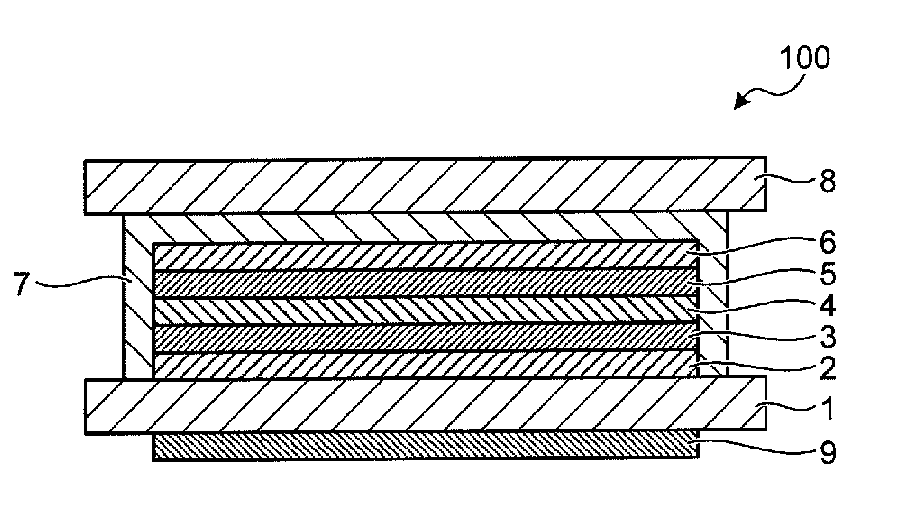
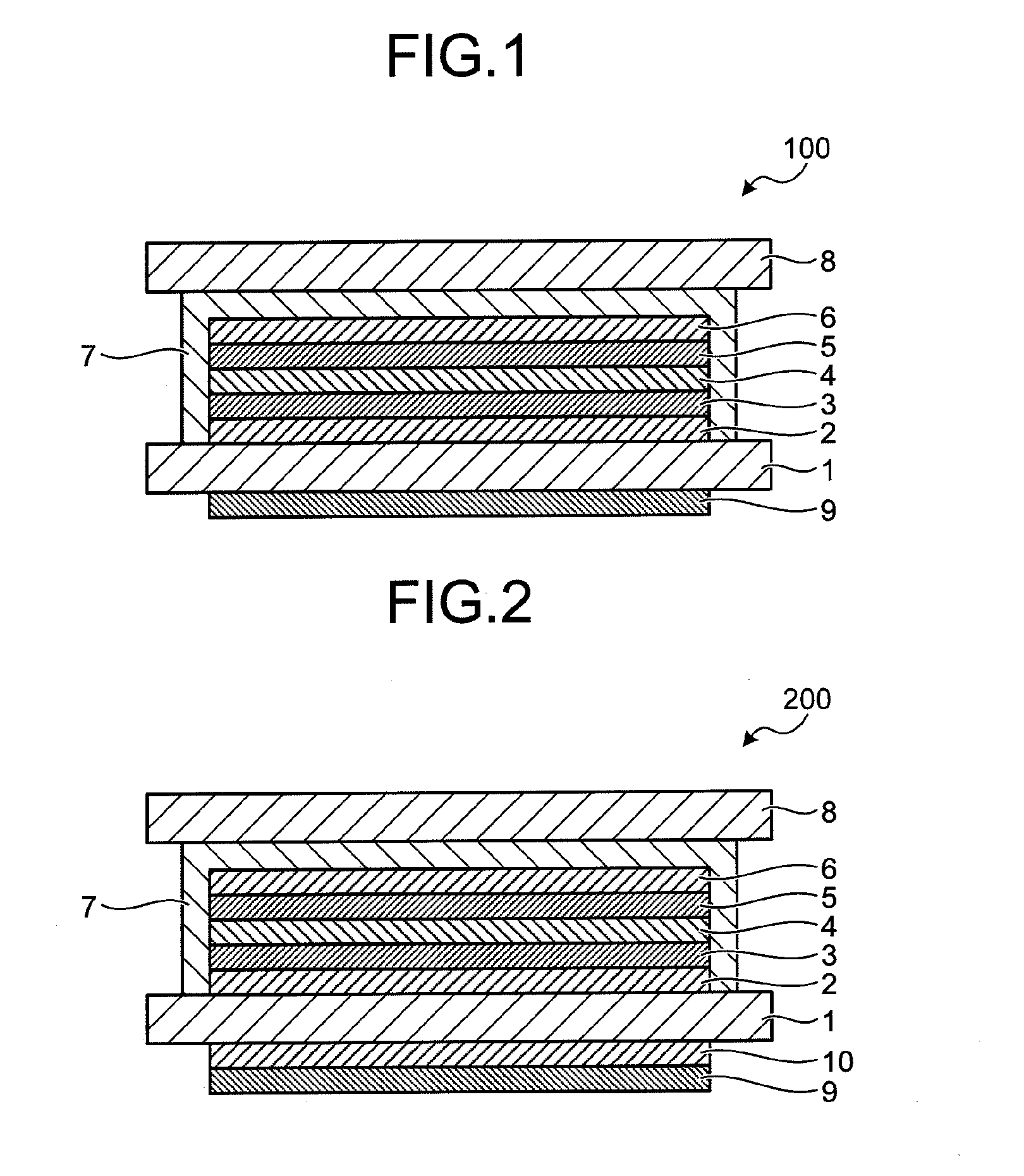
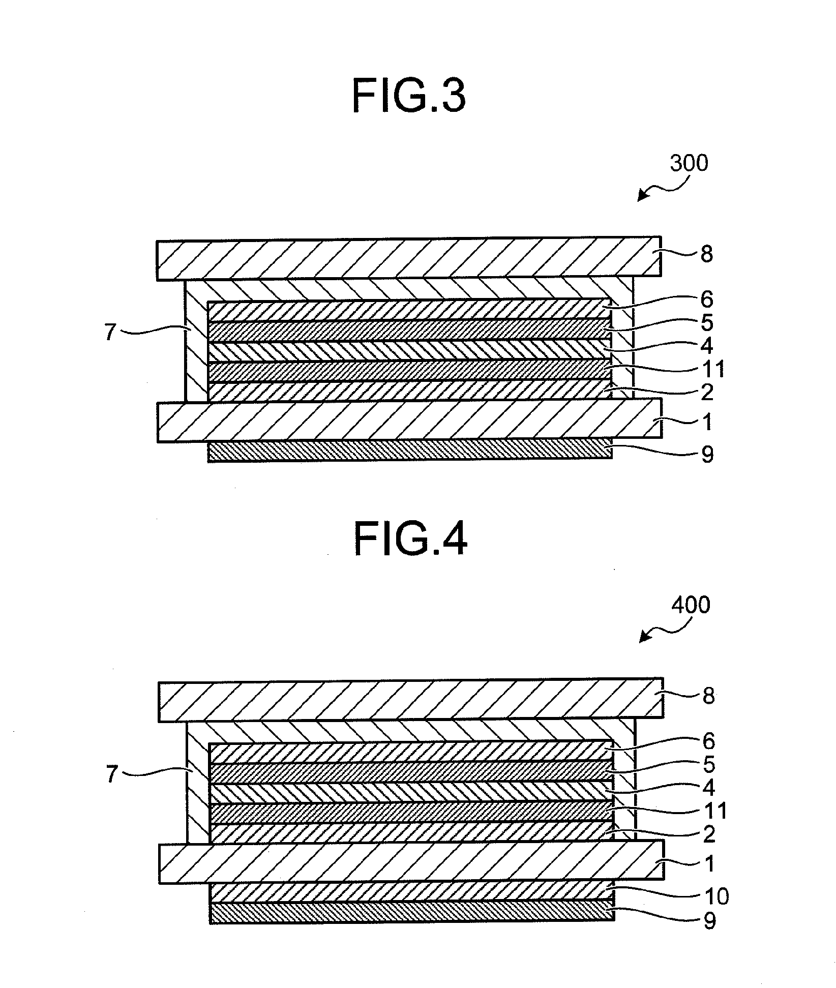
[0149]An organic photovoltaic cell 300 illustrated in FIG. 3 comprises, on a substrate 1, a second electrode 2 serving as the anode, a functional layer 11 comprising an ultraviolet absorber and serving as the electron transport layer, an active layer 4 capable of generating a charge by the input of visible light, a functional layer 5 serving as the hole transport layer, and a first electrode 6 serving as the cathode in this order. Each of the first electrode 6 and the second electrode 2 is connected with a terminal not illustrated in the schematic for extracting electricity to the exterior. The second electrode 2, the functional layer 11, the active layer 4, the functional layer 5, and the first electrode 6 are covered with a sealer layer 7 except for the terminals to be sealed, and on the sealer layer 7, a substrate 8 is provided. Beneath the substrate 1, a wavelength conversion layer 9 is provided so as to convert wavelength of the input ultraviolet light in...
fourth embodiment
[9-4. Fourth Embodiment]
[0154]An organic photovoltaic cell 400 illustrated in FIG. 4 comprises an ultraviolet absorbing layer 10 between the substrate 1 and the wavelength conversion layer 9 in the organic photovoltaic cell 300. Thus, the organic photovoltaic cell 400 comprises the substrate 8, the sealer layer 7, the first electrode 6, the functional layer 5, the active layer 4, the functional layer 11, the second electrode 2, the substrate 1, the ultraviolet absorbing layer 10, and the wavelength conversion layer 9 in this order.
[0155]The organic photovoltaic cell 400 has the structure as mentioned above. Hence, when light is applied from below in the drawing, in a similar manner to that in the first embodiment, visible light in the applied light and visible light that is generated from ultraviolet light by wavelength-conversion in the wavelength conversion layer 9 are input to the active layer 4, thus generating charges in the active layer 4. The charges are extracted from the fi...
example 1
[0174]A glass substrate to which an ITO film having a thickness of 150 nm was attached by a sputtering method as an anode (second electrode) was prepared.
[0175]Onto the ITO film, a dispersion liquid (manufactured by Catalysts & Chemicals Ind. Co., Ltd., trade name: titania sol HPW-10R) dispersing titanium dioxide particles and a dispersant was applied by a spin coating method, and dried at room temperature to form a functional layer (electron transport layer) having a thickness of 70 nm. Here, in the dispersion liquid, the titanium dioxide particles had a diameter of 8 nm to 13 nm, the titanium dioxide had an electrical conductivity of 24.6 mS / cm, the solvent in the dispersion liquid was water, and the dispersion liquid had a pH of 1.3. The titanium dioxide was an ultraviolet absorber capable of absorbing light having a wavelength of 411 nm or smaller.
[0176]Next, an ortho-dichlorobenzene solution comprising a macromolecular compound A that was an alternating polymer of the monomer r...
PUM
| Property | Measurement | Unit |
|---|---|---|
| Efficiency | aaaaa | aaaaa |
| Wavelength | aaaaa | aaaaa |
Abstract
Description
Claims
Application Information


