Solar Cell

Inactive Publication Date: 2011-10-20
RIKEN
View PDF6 Cites 3 Cited by
  • Summary
  • Abstract
  • Description
  • Claims
  • Application Information

AI Technical Summary

Benefits of technology

[0012]The solar cell of the present invention enables to dramatically improve the conversion efficiency per photon absorbed, in the following manner. Specifically, in the process of carriers having energy exceeding the Mott gap being relaxed

Problems solved by technology

However, there are no detailed theoretical studies on the electron behavior during a metal-insulator phase transition induced by light irrad

Method used


Image

  • Solar Cell
  • Solar Cell
  • Solar Cell

Examples


Example

Embodiment 1

[0022]Hereinafter, an embodiment of the present invention will be described in detail on the basis of the drawings.

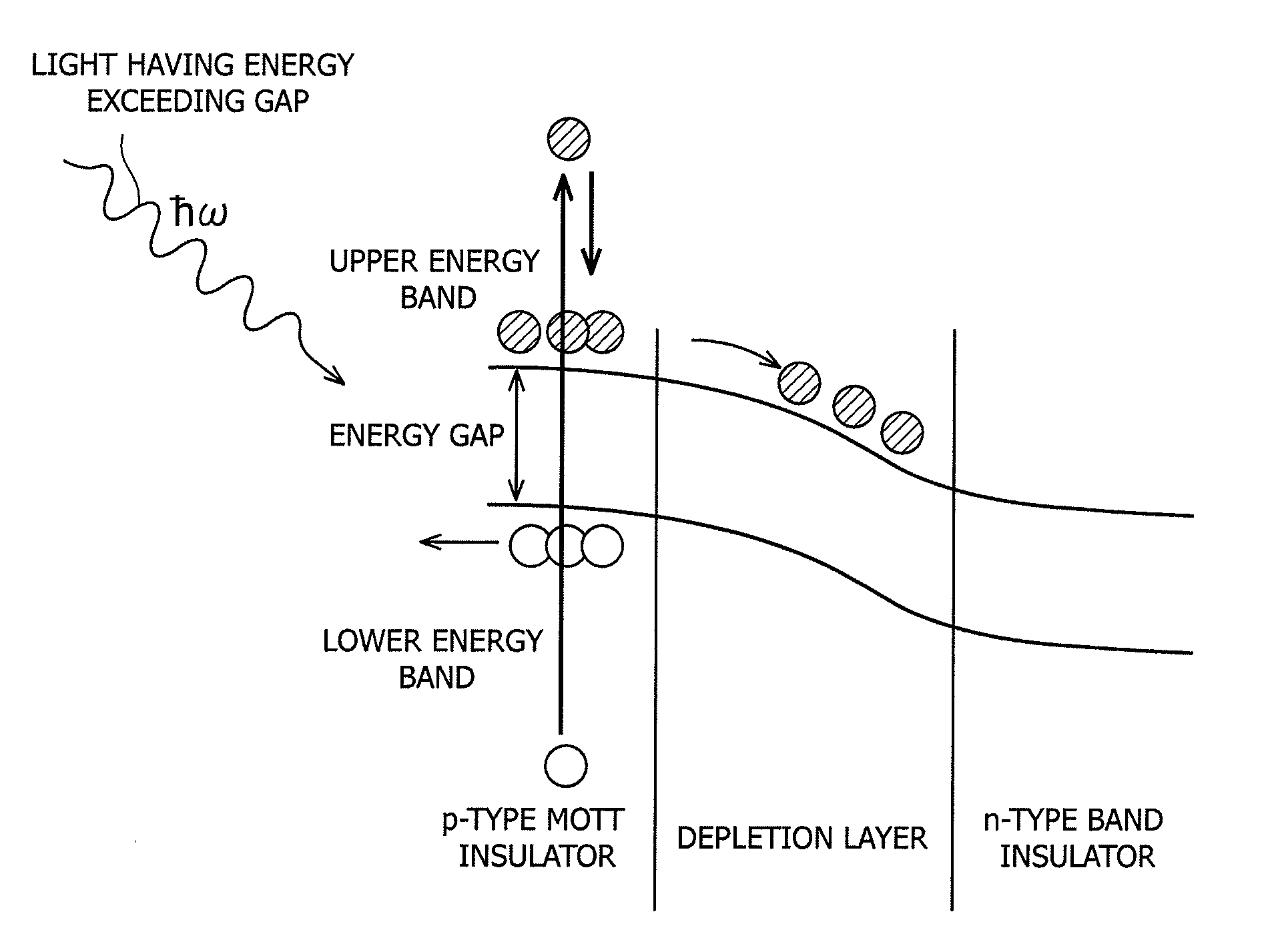
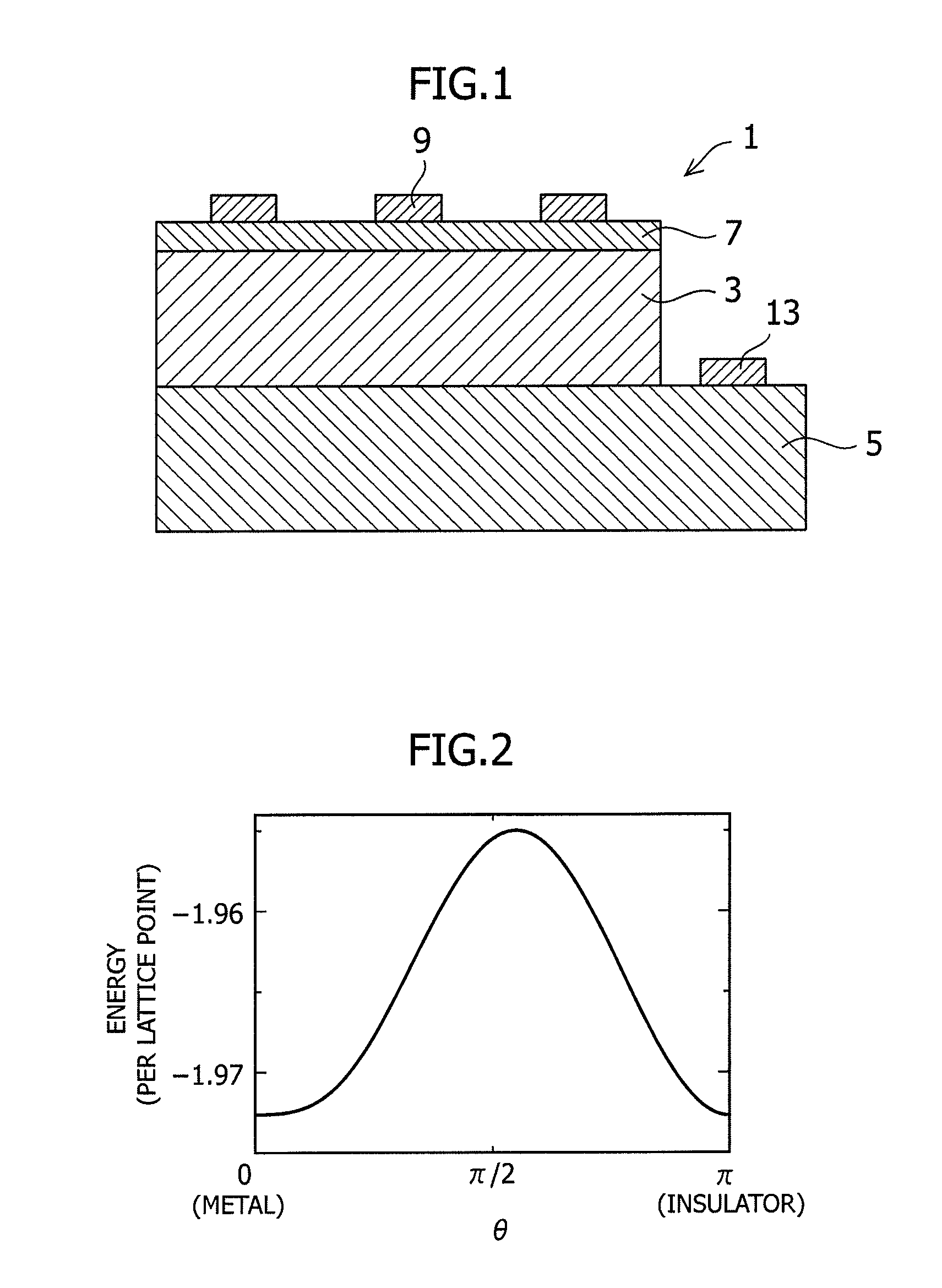
[0023]In a mode shown in FIG. 1, a solar cell 1 comprises a first electrode 7 formed on a sunlight-receiving surface; a first solid material layer 3 formed of a p-type or n-type insulator or a p-type or n-type semiconductor under the first electrode 7; a second solid material layer 5 is formed of an insulator or semiconductor of a type different from that of the first solid material layer 3 under the first solid material layer 3; the two layers 3 and 5 form a p-n junction; and the second solid material layer 5 also has a function of an electrode. Here, at least one of the first and second solid materials is a Mott insulator or a Mott semiconductor.

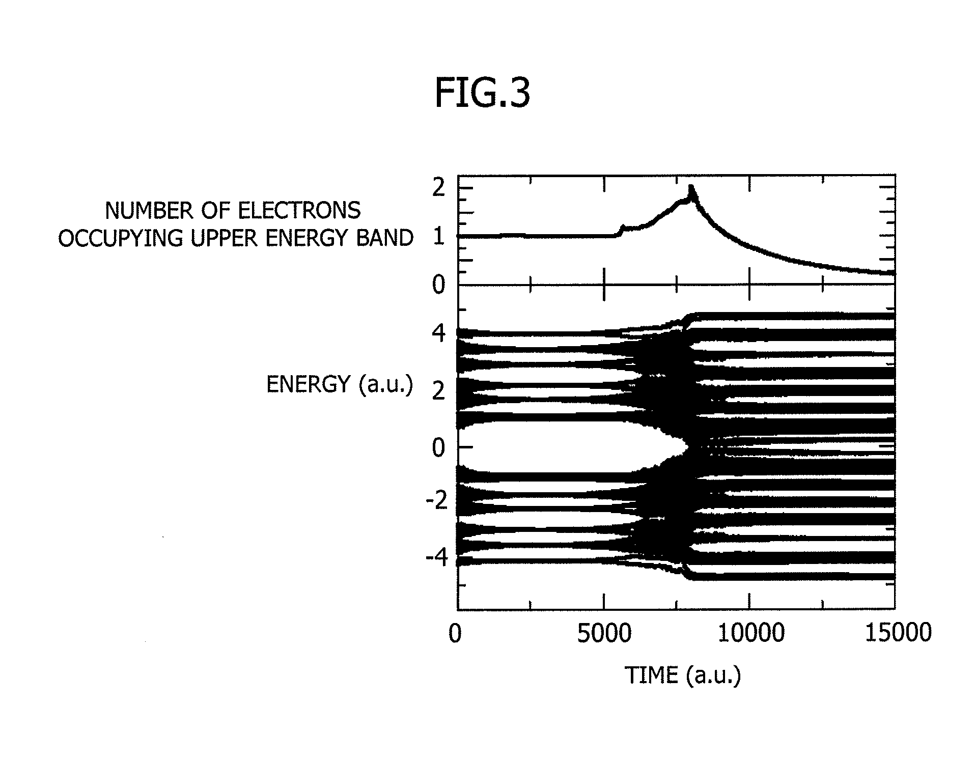
[0024]When such a solar cell is employed, the state of electrons excited by sunlight is totally different from that of excited electrons in conventional cases. This is because almost all Mott insulators or Mott sem...

Example

Embodiment 2

[0067]On the basis of the above-described simulation example, a solar cell as shown in FIG. 1 was fabricated in which a p-n junction was formed of a p-type Mott insulator and an n-type band semiconductor. First, an n-type band semiconductor, Nb;SrTiO3 crystal, was used as the substrate 5, which was designed to serve also as a lower electrode. On the substrate 5, a p-type Mott insulator LaMnO3, was formed by the laser ablation method in a thickness of 300 A. The film was formed under the conditions of 850° C. and 1 mTorr in an oxygen atmosphere at a growth rate of 16 A / minute. Subsequently, a gold thin film having a thickness of 50 A was formed as the upper electrode (the first electrode) 7, and then a heat treatment was conducted at 450° C. and 1 atm in an oxygen atmosphere. An auxiliary electrode 11 (200A) was formed on the lower substrate 5 by using titanium metal. FIG. 7 shows photo-current-voltage characteristics observed when the solar cell 1 using the Mott insulato...


PUM


Abstract

A solar cell 1 has a p-n junction structure between a first solid material layer 3 comprising an insulator or a semiconductor and a second solid material layer 5 comprising an insulator or a semiconductor of a type different from the type of the first solid material layer 3, in which structure a Mott insulator or a Mott semiconductor is used as a solid material of at least one of the layers.

Description

BACKGROUND OF THE INVENTION[0001]1. Field of the Invention[0002]The present invention relates to a solar cell, and particularly to a solar cell using a phenomenon that is unique to a strongly correlated electron system, the phenomenon being discovered in a transition process of a Mott insulator or a Mott semiconductor to a metal phase upon light irradiation is applied.[0003]2. Description of the Related Art[0004]Silicon element, gallium-arsenic compound semiconductors, and the like are presently used as a material exhibiting solar cell functions. The principle of photovoltaic energy conversion in these materials involves the use of single-electron excitation induced by photons as shown in FIG. 8. A solar cell utilizing the single-electron excitation has such a limitation that one electron is excited by one photons. Carriers (electrons and holes) receiving an energy exceeding the band gap undergo only heat dissipation, until the carriers reach the band edge. Accordingly, in principle...

Claims


Application Information

Patent Timeline
IPC IPC(8): H01L31/02
CPCH01L31/0264H01L31/0296H01L31/0304H01L31/0336H01L31/072Y02E10/549H01L31/18H01L51/0084H01L51/0087H01L51/4206Y02E10/544H01L31/0725H10K85/341H10K85/346H10K30/451
Inventor KOSHIBAE, WATARUNAKAMURA, MASAOKAWASAKI, MASASHINAGAOSA, NAOTOTAGUCHI, YASUJIROTOKURA, YOSHINORIFURUKAWA, NOBUO
Owner RIKEN
Why Eureka
Try Eureka