

Nitride semiconductor-based solar cell and manufacturing method thereof
Inactive Publication Date: 2014-01-02
GWANGJU INST OF SCI & TECH
View PDF4 Cites 5 Cited by
- Summary
- Abstract
- Description
- Claims
- Application Information
AI Technical Summary
Benefits of technology
The present invention provides a photoelectric device with improved efficiency. This is achieved by the use of a mask layer with opening parts, through which first layers of n-type nitride semiconductor are exposed. These layers penetrate through the opening parts and form hexagonal pyramid shapes, which increase the area of the photoactive layer receiving incident light. As a result, photoelectric conversion efficiency is improved.
Problems solved by technology
However, it has disadvantages in that a high cost is required to generate electricity, such that an economical efficiency is low, and a power generation amount is limited due to a weather condition and a limited sunshine time.
In these structures, an excessive etching process is introduced, such that a complicated manufacturing process is required.
However, there are still problems such as a complicated manufacturing process, deformation of a material of a thin film due to etching, and the like.
Method used
View moreImage
Smart ImageViewing Examples

Examples
Embodiment Construction
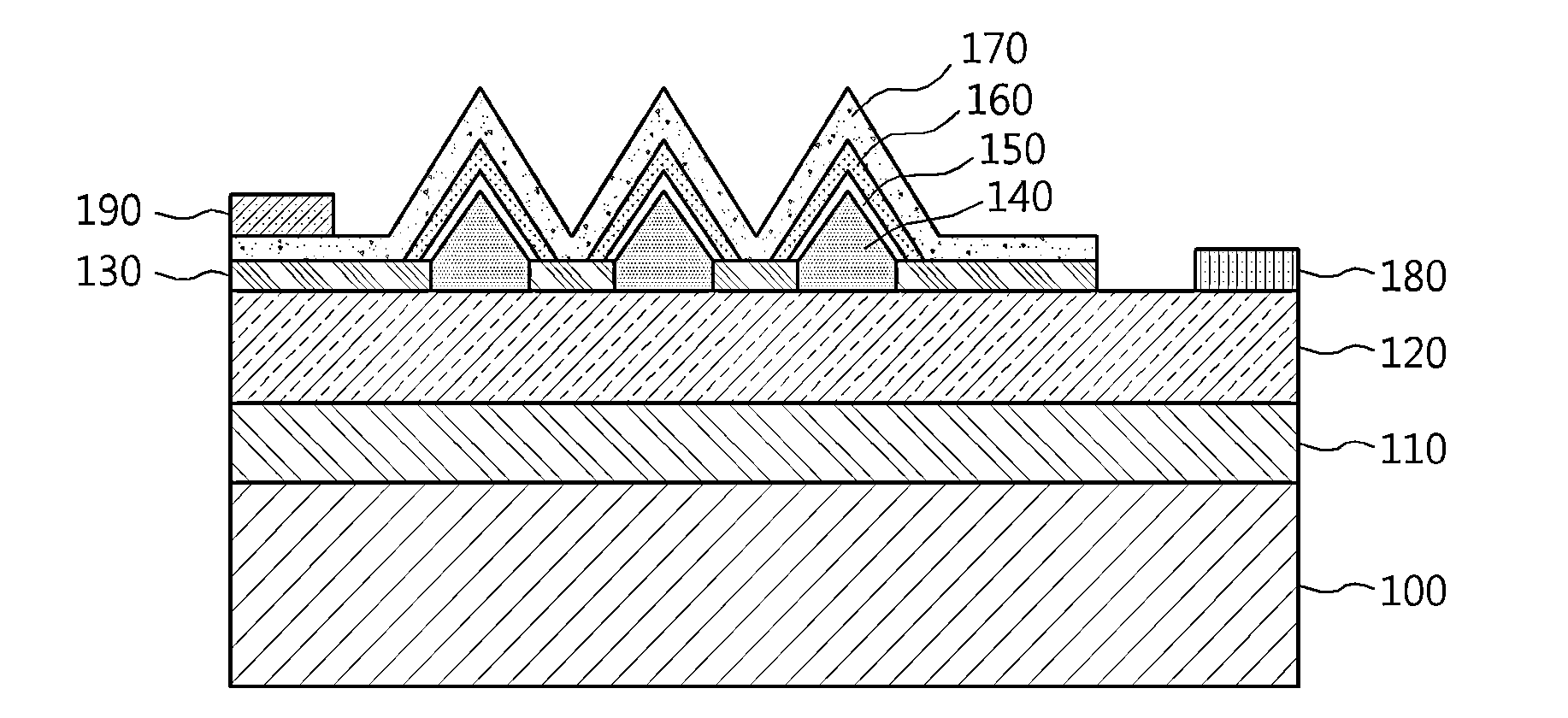
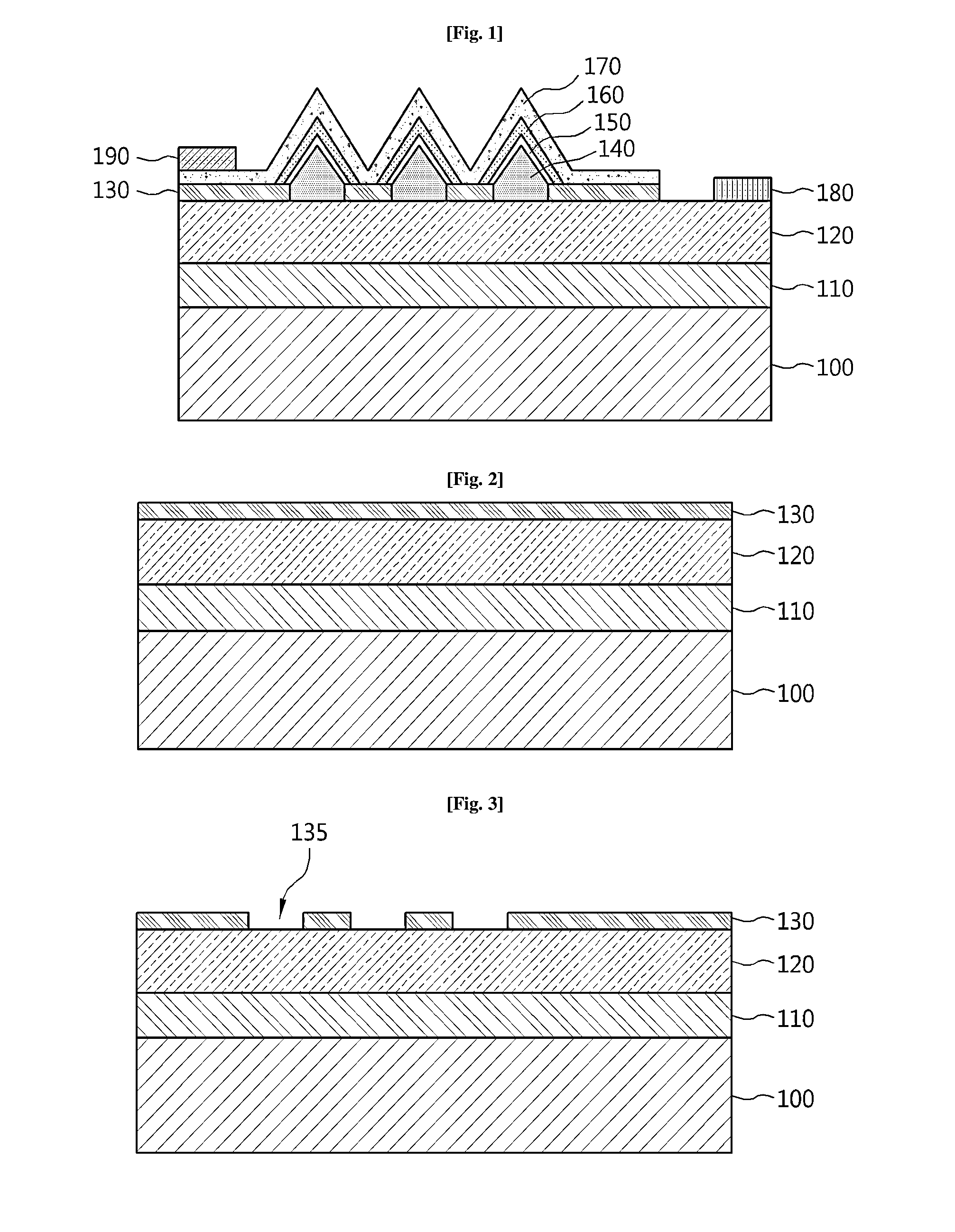
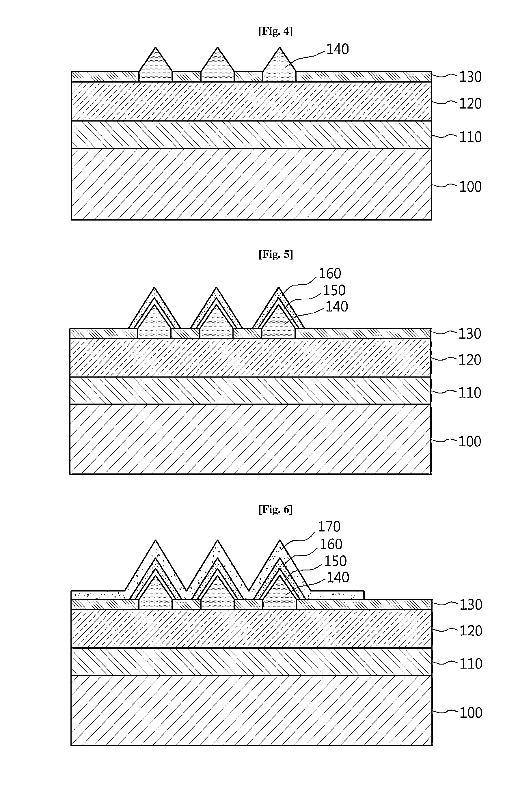
of Main Elements]100: Substrate110: Buffer layer120: First n-type nitride semiconductor layer140: Second n-type130: Mask layernitride semiconductor layer150: Photoactive layer160: P-type nitride170: Transparent electrodesemiconductor layer
Login to View More PUM
 Abstract
Disclosed herein are a nitride semiconductor-based solar cell including a photoactive layer having a wide area for incident light and a manufacturing method thereof. Opening parts are formed in a mask layer partially shielding a first n-type nitride semiconductor layer. The first n-type nitride semiconductor layer is exposed through the opening part, and second n-type nitride semiconductor layers are grown based on the exposed first n-type nitride semiconductor layer. The grown second n-type nitride semiconductor layer is buried in the opening part and is formed in a hexagonal pyramid shape. In addition, a photoactive layer and a p-type nitride semiconductor layer are sequentially formed along the second n-type nitride semiconductor layer. Therefore, a hole injection-electron pair is easily formed by the incident light. Further, an area of the photoactive layer is increased, such that photoelectric conversion efficiency is improved.
Description
TECHNICAL FIELD [0001]The present invention relates to a solar cell, and more particularly, to a solar cell including a nitride semiconductor grown on an intended region.BACKGROUND ART [0002]A solar cell is a system directly converting solar energy into electrical energy using a photovoltaic effect. This photovoltaic power generation has advantages in that it does not require a fuel and does not cause thermal pollution and environmental pollution. However, it has disadvantages in that a high cost is required to generate electricity, such that an economical efficiency is low, and a power generation amount is limited due to a weather condition and a limited sunshine time.[0003]A key point of a solar cell technology is to allow sunlight having energy larger than that of a forbidden band to be incident to a semiconductor device formed by a p-n junction, thereby forming a hole-electron pair. In the formed hole-electron pair, the electron moves to an n-type semiconductor layer and the hol...
Claims
Login to View More Application Information
Patent Timeline
 IPC IPC(8): H01L31/0236H01L31/18
CPCH01L31/02363H01L31/1856H01L31/03529H01L31/03044H01L31/035236H01L31/075Y02E10/544Y02E10/548B82Y20/00H01L31/04H01L31/0236
InventorLEE, DONG SEONBAE, SI YOUNGKIM, DO HYUNGBAEK, JONG HYEOBLEE, SEUNG-JAE
OwnerGWANGJU INST OF SCI & TECH