Photoelectric conversion apparatus

Inactive Publication Date: 2014-10-02
KYOCERA CORP
View PDF5 Cites 1 Cited by
  • Summary
  • Abstract
  • Description
  • Claims
  • Application Information

AI Technical Summary

Benefits of technology

[0009]The above embodiment provides a photoelectric c

Problems solved by technology

However, with mechanical scribing, described above, the photoelectric conversion layer may be incompletely removed from the lower electrode layer and remain on the low

Method used


Image

  • Photoelectric conversion apparatus
  • Photoelectric conversion apparatus
  • Photoelectric conversion apparatus

Examples


Example

[0021]A photoelectric conversion device according to an embodiment of the present invention will now be described in detail with reference to the drawings.

Structure of Photoelectric Conversion Device

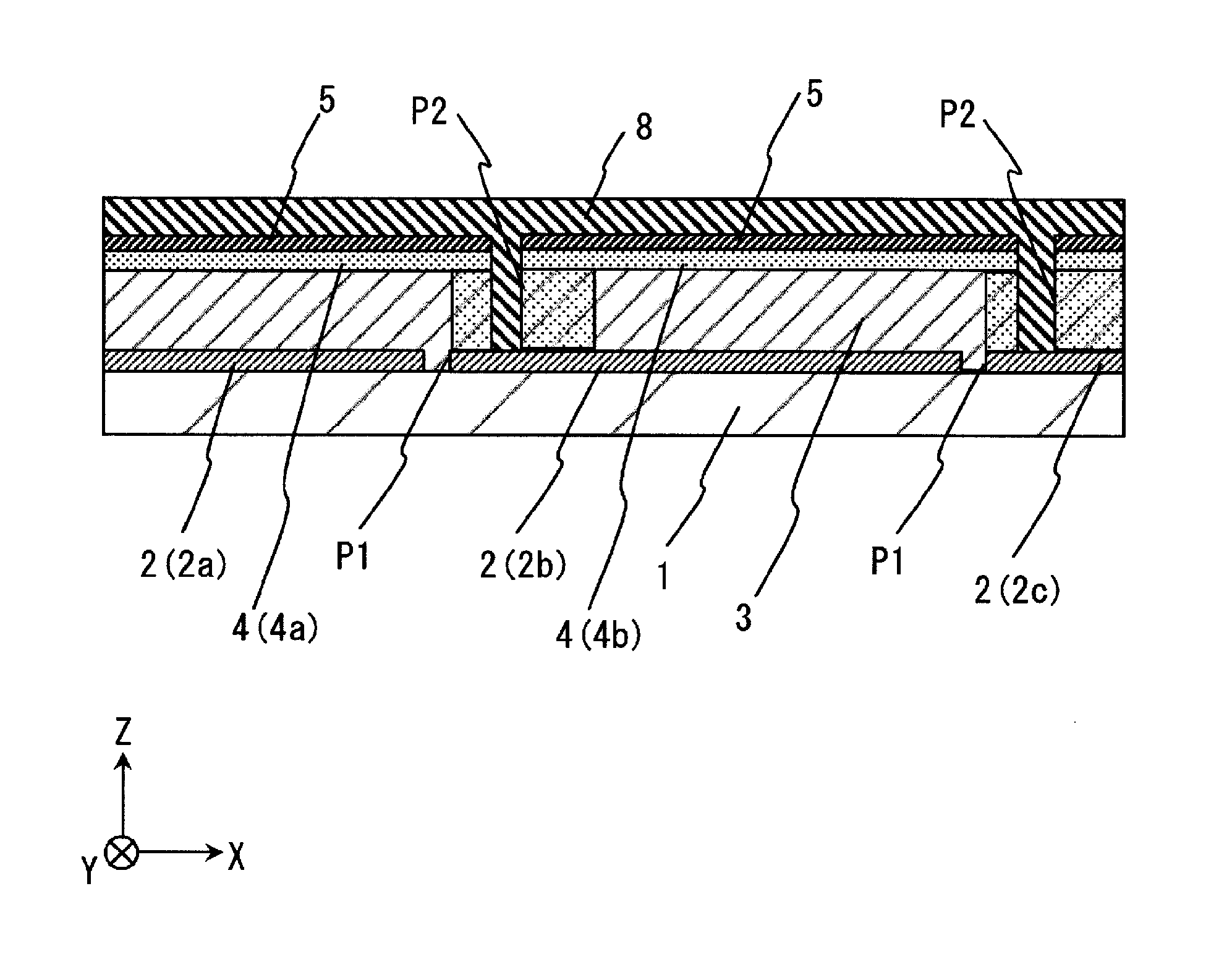
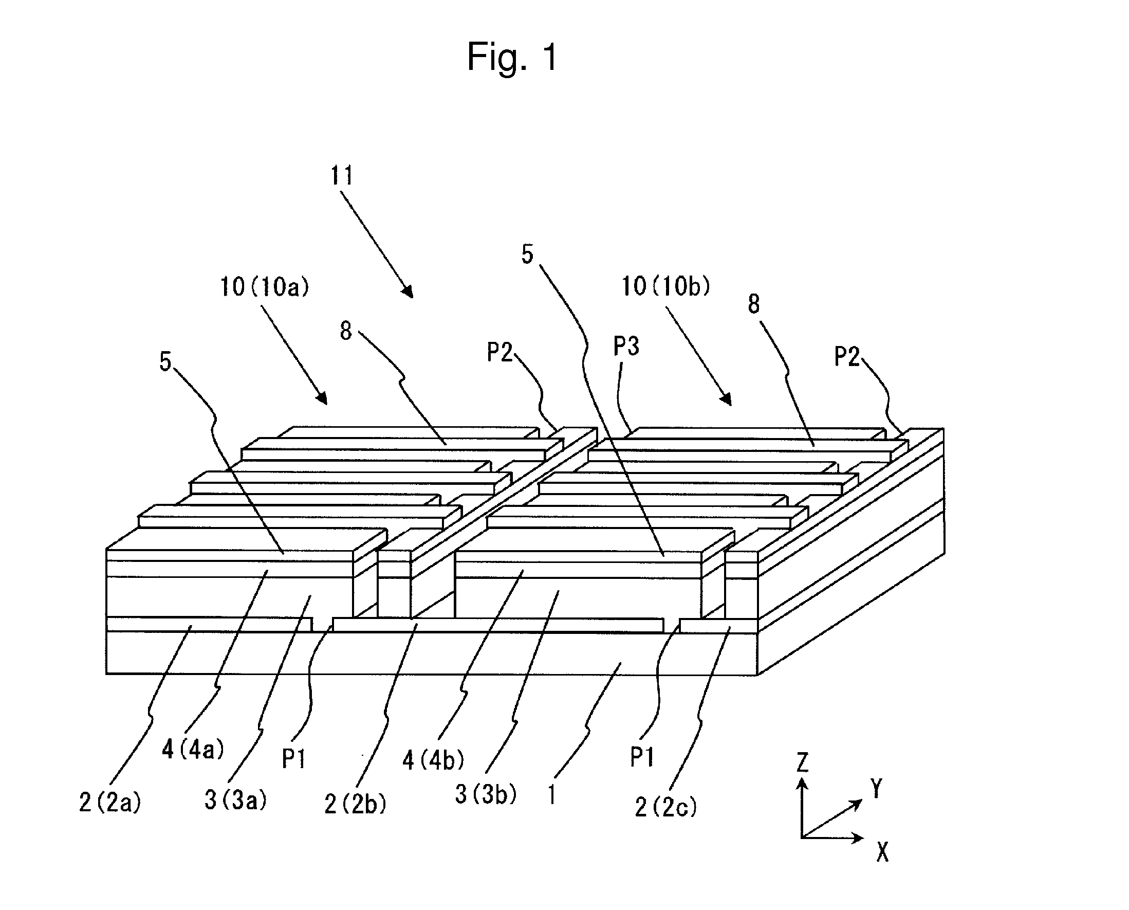
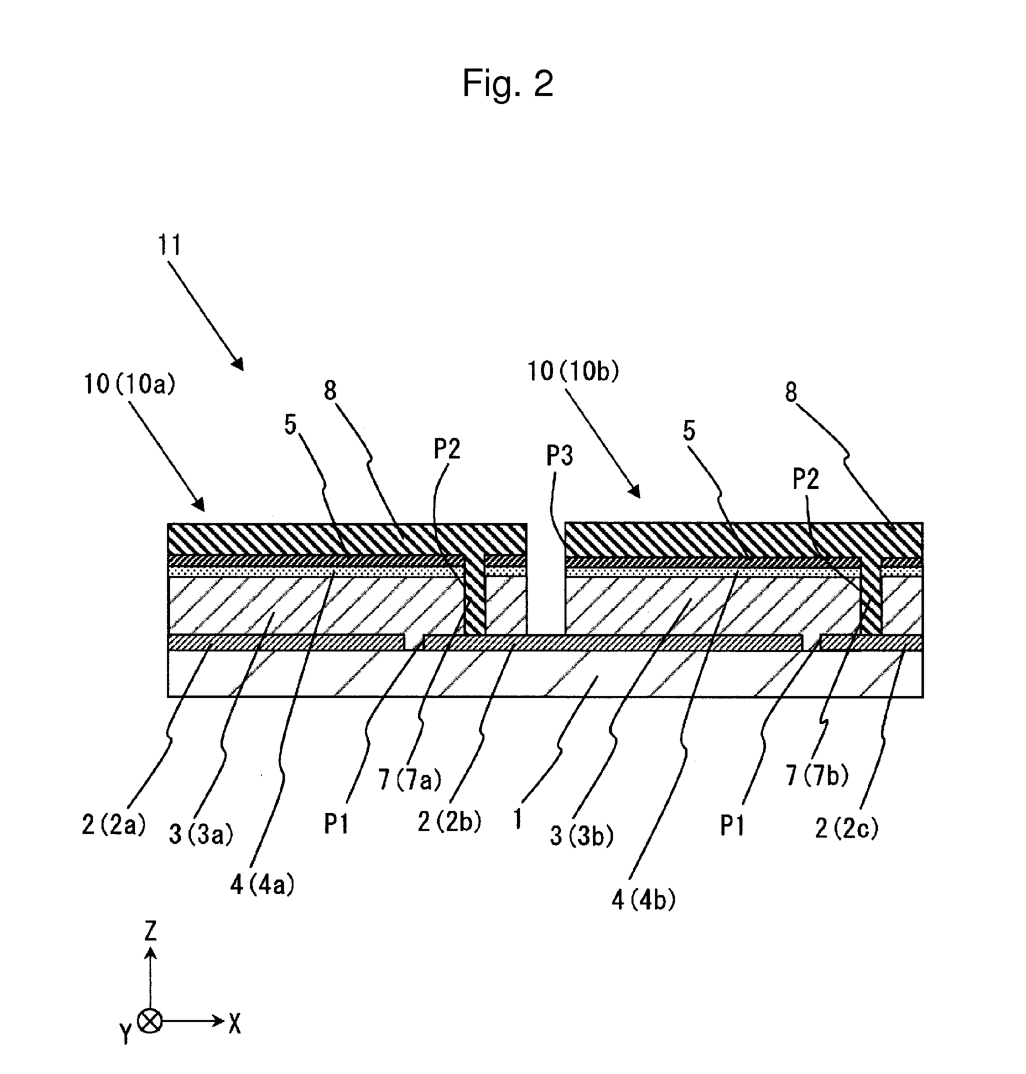
[0022]FIG. 1 is a perspective view showing an example of a photoelectric conversion device according to an embodiment of the present invention. FIG. 2 is an X-Z sectional view of the photoelectric conversion device 11 in FIG. 1. In FIGS. 1 and 2, a right-hand XYZ coordinate system is shown in which the X-axis direction is the direction in which photoelectric conversion cells 10 are arranged (the left-to-right direction as viewed in FIG. 1).

[0023]The photoelectric conversion device 11 includes a plurality of photoelectric conversion cells 10 arranged on a substrate 1 and electrically connected to each other. Although only two photoelectric conversion cells 10a and 10b are shown in FIG. 1 for illustration purposes, the photoelectric conversion device 11 may in practice include a large num...


PUM


Abstract

A photoelectric conversion device is disclosed. The photoelectric conversion device includes: first and second electrode layers on a main surface of a substrate, separated by a space; a first semiconductor layer having a first conductivity type and containing crystal grains; a second semiconductor layer on the first semiconductor layer, having a second conductivity type different from the first conductivity type; and one or more first connection conductors on the second electrode layer, coupled to a side of the second semiconductor, and electrically connecting the second semiconductor layer to the second electrode layer. The first semiconductor layer includes: a first portion on the first electrode layer, including crystal grains having a first average size; a second portion disposed at the space on the substrate; and a third portion on the second electrode layer, including crystal grains having a second average size that is larger than the first average size.

Description

TECHNICAL FIELD[0001]The present invention relates to photoelectric conversion devices including a plurality of photoelectric conversion cells connected together.BACKGROUND ART[0002]Some photoelectric conversion devices for applications such as solar energy generation include a photoelectric conversion layer made of a chalcopyrite-type group I-III-VI compound semiconductor such as CIGS, which has a high optical absorption coefficient. Such photoelectric conversion devices are disclosed in, for example, Japanese Unexamined Patent Application Publication Nos. 2000-299486 and 2002-373995. CIGS, which has a high optical absorption coefficient, is suitable for forming a thinner and larger photoelectric conversion layer at a lower cost, and research and development has been directed to the use of CIGS for next-generation solar cells.[0003]A chalcopyrite-type photoelectric conversion device includes a plurality of photoelectric conversion cells arranged side by side in a plane, each includ...

Claims


Application Information

Patent Timeline
IPC IPC(8): H01L31/0368H01L31/05H01L31/032
CPCH01L31/0368H01L31/05H01L31/0322Y02E10/50H01L31/0465
Inventor UMESATO, KAZUMASAHASHIMOTO, YUKARIISHIKAWA, SHINYA
Owner KYOCERA CORP
Why Eureka
Try Eureka