High voltage wire bond free leds

a technology of leds and high voltage, applied in the field of led chips, can solve the problems of limited current levels, chip unusability, and high current operation necessitate relatively expensive drivers,

Active Publication Date: 2011-04-14
CREELED INC
View PDF67 Cites 96 Cited by
  • Summary
  • Abstract
  • Description
  • Claims
  • Application Information

AI Technical Summary

Benefits of technology

[0012]The present invention provides various embodiments of semiconductor devices and LED chips that are high voltage and wire bond free. The different embodiments comprise various arrangements having a number of sub-LEDs on a submount, the sub-LEDs formed from a single junction LED, and interconnections connecting these sub-LEDs.

Problems solved by technology

One disadvantage of this approach is that at the systems level high current operation necessitates relatively expensive drivers to provide the constant DC current source for such components.
Further, there can be limits to the level of current that can be applied to these LED chips and if the single junction fails, the chip can be unusable.
However, the lower driver cost for such solutions can be outweighed by the high cost of the multiple individual components.
These LED array solutions can be less compact than desired as they provide for extended non-light emitting “dead space” between adjacent LED packages and cavities.
This dead space provides for larger devices, and can limit the ability to shape the output beam by a single compact optical element like a collimating lens or reflector into a particular angular distribution.
This makes the construction of solid state lighting luminares that provide for directed or collimated light output within the form factor of existing lamps (or even smaller) difficult to provide.
This can present challenges in providing a compact LED lamp structure incorporating an LED component that delivers light flux levels in the 1000Lumen and higher range from a small optical source.
The use of wire bonds, however, can be a disadvantageous because of their fragility.
In addition, wire bonding can negatively impact light emission and detract from the physical appearance of LEDs when they are not emitting light.

Method used


Image

  • High voltage wire bond free leds
  • High voltage wire bond free leds
  • High voltage wire bond free leds

Examples


Embodiment Construction

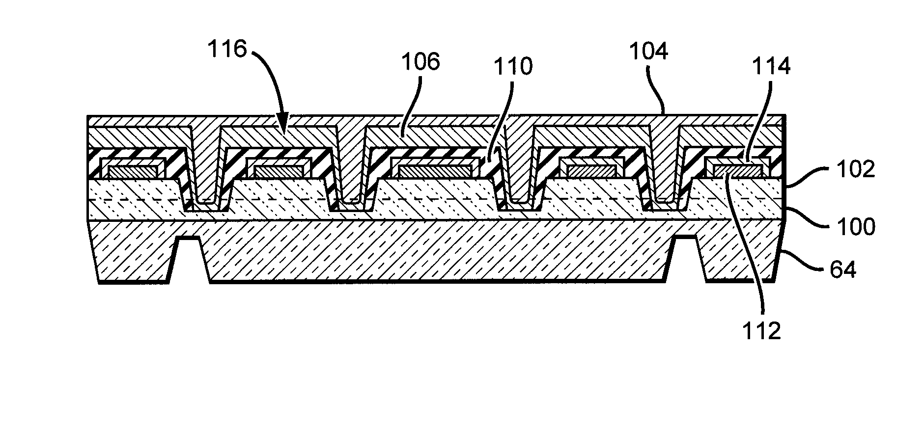
[0030]The present invention comprises a monolithic LED chip or component having a plurality of LED junctions or sub-LEDs mounted onto a substrate or submount (“submount”) to create a single compact optical source element. As used in the present application, monolithic refers to LED chips wherein the emitters are mounted on one substrate or submount. According to the present invention, at least some of the junctions or sub-LEDs are arranged on the submount, with different embodiments providing multiple series interconnections, or combinations of series / parallel interconnections. The LED chips according to the present invention can emit different colors of light, with some embodiments emitting white light.

[0031]In one embodiment, an LED chip is provided having the same dimensions or footprint as a conventional high output single junction LED that uses low voltage and high current operation to provide high luminous flux operation. In some embodiments the active area of this type of con...


PUM


Abstract

An LED chip and method of fabricating the same is disclosed that comprises a plurality of sub-LEDs, said sub-LEDs interconnected such that the voltage necessary to drive said sub-LEDs is dependent on the number of said interconnected sub-LEDs and the junction voltage of said sub-LEDs. Each of said interconnected sub-LEDs comprising an n-type semiconductor layer, a p-type semiconductor layer, and an active or quantum well region interposed between the n-type and p-type layers. The monolithic LED chip further comprising a p-electrode having a lead that is accessible from a point on a surface opposite of a primary emission surface of the monolithic LED chip, the p-electrode electrically connected to the p-type layer, and an n-electrode having a lead that is accessible from a point on the surface opposite of the primary emission surface, the n-electrode electrically connected to the n-type layer. These sub-LEDs interconnected by at least a metallization layer on the n-type and p-type layers, which is insulated so that it does not short the sub-LEDs. Further, the LED chip is capable of being electrically coupled for operation without wire bonds.

Description

RELATED APPLICATIONS[0001]This is a continuation in part application from Ser. No. 12 / 418,816 filed Apr. 6, 2009, entitled “High Voltage Low Current Surface-Emitting LED”, and application Ser. No. 11 / 985,410 filed Nov. 14, 2007, entitled “Wire Bond Free Wafer Level LED.”BACKGROUND OF THE INVENTION[0002]1. Field of the Invention[0003]This invention relates to light emitting diode (LED) chips and in particular LED chips having multiple series connected junctions interconnected to allow for high voltage and low current operation and capable of wire bond free fabrication and operation.[0004]2. Description of the Related Art[0005]Light emitting diodes (LED or LEDs) are solid state devices that convert electric energy to light, and generally comprise one or more active layers of semiconductor material sandwiched between oppositely doped layers. When a bias is applied across the doped layers, holes and electrons are injected into the active layer where they recombine to generate light. Lig...

Claims


Application Information

Patent Timeline
Patent Type & Authority Applications(United States)
IPC IPC(8): H01L33/32H01L33/00
CPCH01L27/153H01L2224/32257H01L33/20H01L33/22H01L33/38H01L33/405H01L33/62H01L2224/48091H01L2224/73265H01L27/156H01L2224/48247H01L2224/48227H01L2224/32245H01L2924/01087H01L2924/00014H01L2924/00H01L2924/00012
Inventor YAO, ZHIMIN JAMIE
Owner CREELED INC
Why Eureka
Try Eureka