Photoelectric sensor, display panel and display device

A photoelectric sensor and display panel technology, applied in the field of display panels, display devices, and photoelectric sensors, can solve the problems that photoelectric sensors cannot be applied and are not easy to detect.

Inactive Publication Date: 2017-07-07
BOE TECH GRP CO LTD
View PDF7 Cites 5 Cited by
  • Summary
  • Abstract
  • Description
  • Claims
  • Application Information

AI Technical Summary

Problems solved by technology

[0003] Found in practical applications using existing photoelectric sensors: see image 3 , image 3 The abscissa in the graph represents the brightness corresponding to the light intensity, and the ordinate represents the leakage current. Different curves 1-4 correspond to the turn-on voltages of different phototransistors (curves 1-4 correspond to turn-on voltages of 0V~3V), from image 3 It can be seen that the leakage current changes with the intensity of the light source. For example, when the light intensity is low, the leakage current changes relatively large with the change of the light intensity, so it can be detected; however, in Larger light intensity (for example: the corresponding brightness is 4000cd / m 2 Above) the change of the leakage current is small with the increase of the light intensity, therefore, it is not easy to be detected
[0004] Therefore, the existing photoelectric sensor cannot be applied under high light intensity, therefore, there is an urgent need for a photoelectric sensor that can be applied under high light intensity.

Method used


Image

  • Photoelectric sensor, display panel and display device
  • Photoelectric sensor, display panel and display device
  • Photoelectric sensor, display panel and display device

Examples


Embodiment 1

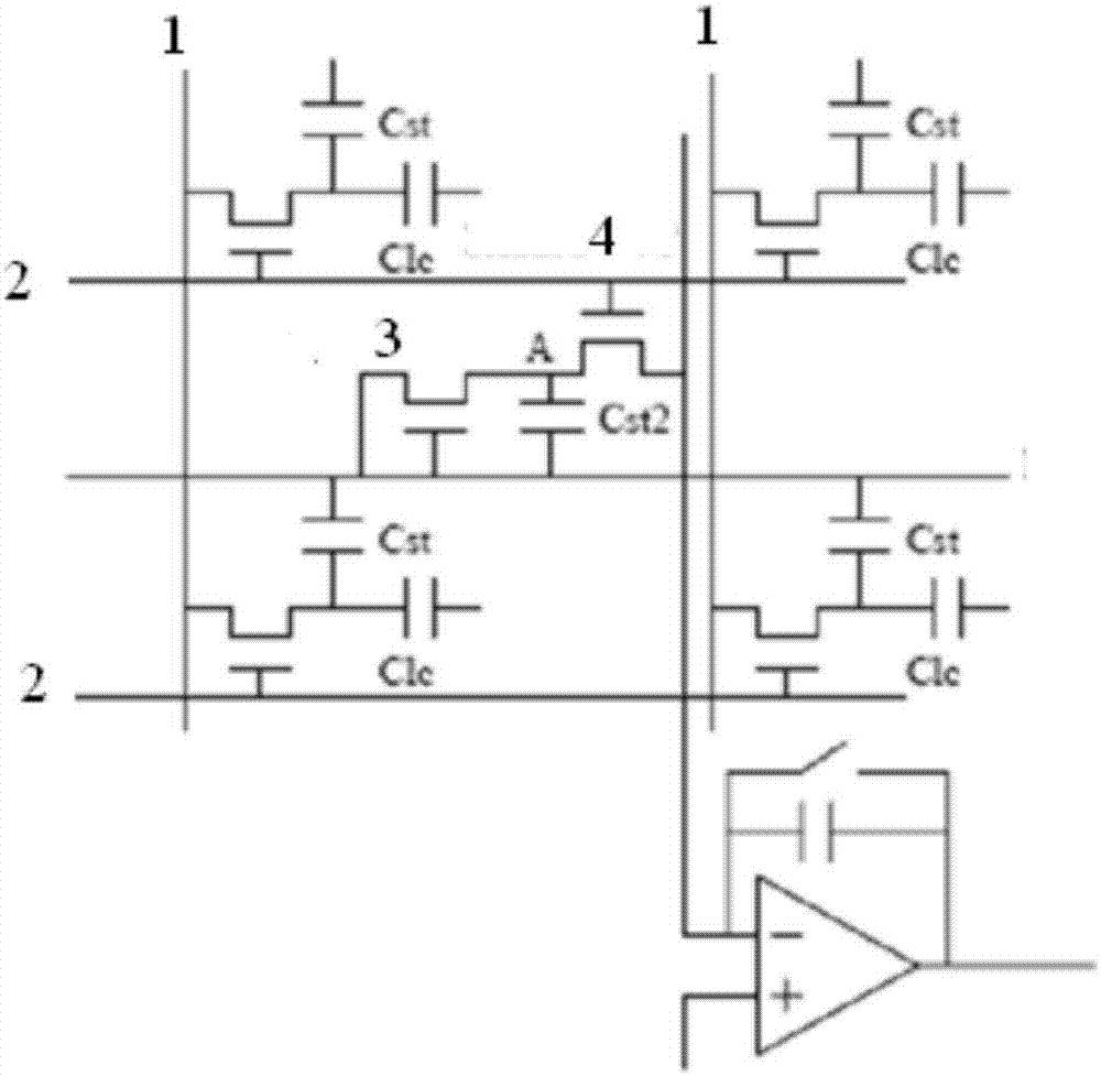
[0030] Figure 4 For the functional block diagram of the photoelectric sensor provided by the embodiment of the present invention, please refer to Figure 4 , the photoelectric sensor provided by the embodiment of the present invention includes: a photoelectric conversion unit 10 and an optical processing layer 20 . Wherein, the photoelectric conversion unit 10 is used to receive an optical signal and convert the optical signal into an electrical signal; the optical processing layer 20 is arranged on the light-incident side of the photoelectric conversion unit 10, and the optical processing layer 20 is used to process the optical signal to reduce the photoelectric conversion The luminous flux of the unit 10, so that the leakage current converted by the photoelectric conversion unit 10 can be accurately detected.

[0031] In the present invention, since the optical processing layer 20 is arranged in the photoelectric sensor, it is used to process the optical signal, so as to r...

Embodiment 2

[0046] An embodiment of the present invention also provides a display panel, including the photoelectric sensor provided in Embodiment 1 above.

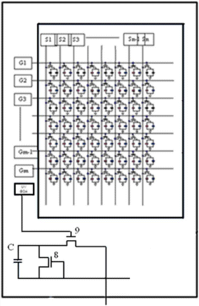
[0047] Preferably, the display panel includes at least one photosensitive region, and at least one photosensitive region includes a plurality of photosensors with different optical processing layers, so that different photosensors can accurately measure different light intensity ranges, so that the Increases the range of light intensity that the display panel can accurately measure.

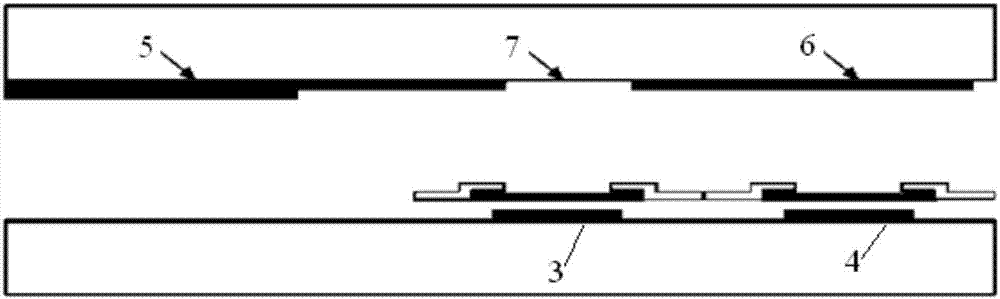
[0048] Specifically, when the optical processing layer of the photosensor is a light-shielding layer, the light-shielding areas of the photoelectric conversion unit 10 shielded by the multiple light-shielding layers are different. More specifically, as Image 6 As shown, the photosensitive region includes photoelectric sensors (respectively 1-5) with a quantity of 5 different optical processing layers 20. Since the radial dimension of the photoelectric...

Embodiment 3

[0052] An embodiment of the present invention also provides a display device, including the display panel provided above in the present invention.

[0053] Among them, display devices include but are not limited to: mobile phones, tablet computers, televisions, monitors, notebook computers, digital photo frames, navigators and any other products or components with display functions

[0054] The display device provided by the embodiment of the present invention includes the display panel provided by the above-mentioned embodiment of the present invention, so it can be applied in an environment with high light intensity.


PUM


Abstract

The invention provides a photoelectric sensor, which comprises a photoelectric conversion unit used for receiving optical signals and converting the optical signals into electric signals; and an optical processing layer arranged at the light entering side of the photoelectric conversion unit and used for processing the optical signals to reduce luminous flux of light reaching the photoelectric conversion unit. The invention also provides a display panel comprising the photoelectric sensor, and a display device. The photoelectric sensor can be used in high light intensity, so that light intensity range capable of being accurately measured by the display panel and the display device can be improved greatly.

Description

technical field [0001] The invention belongs to the field of display technology, and in particular relates to a photoelectric sensor, a display panel and a display device. Background technique [0002] In an OLED panel, a photo sensor is usually set up for fingerprint recognition, touch control, etc., such as Figure 1a with Figure 1b As shown, the traditional photosensor integrated in the display panel is arranged in a small area of ​​the pixel unit formed by the intersection of the data line 1 and the gate line 2. The photosensor circuit is various, and the mainstream is 2T1C circuit, including: a photoelectric sensor Transistor 3 (photo TFT) and a readout transistor 4 (readout TFT), the phototransistor 3 is used to turn off during the photosensitive period and will always generate leakage current stored in the capacitor C under light; the readout transistor 4 is used for each Periodically open to read out the electric signal stored in the capacitor, and then obtain the ...

Claims


Application Information

Patent Timeline
Patent Type & Authority Applications(China)
IPC IPC(8): H01L31/0216H01L27/32
CPCH01L31/02164H01L31/02165H10K59/60Y02E10/50H10K59/65H01L27/142H01L27/1214H01L27/14H10K59/13H10K59/38
Inventor 吴俊纬贾亚楠刘英明丁小梁王海生董学
Owner BOE TECH GRP CO LTD
Why Eureka
Try Eureka