

Internal wiring structure of semiconductor device
a technology of internal wiring and semiconductor devices, applied in the direction of dc-ac conversion without reversal, solid-state devices, basic electric elements, etc., can solve the problems of increasing the heat generated in the semiconductor chips, high switching loss, and certain limitations in the related art, so as to reduce the mutual inductance and improve the heat dissipation effect
- Summary
- Abstract
- Description
- Claims
- Application Information
AI Technical Summary
Benefits of technology
Problems solved by technology
Method used
Image

Examples
example 1
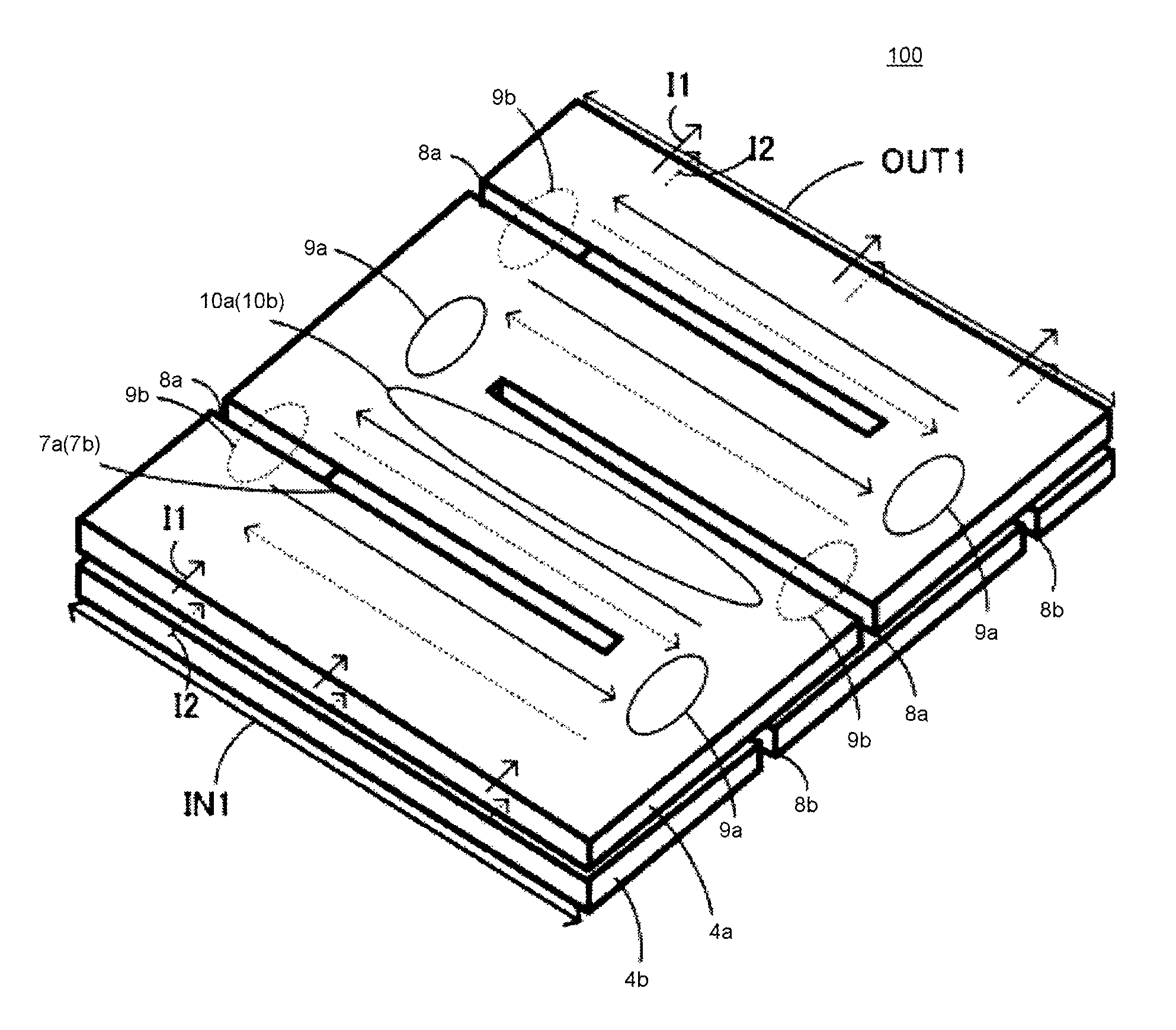
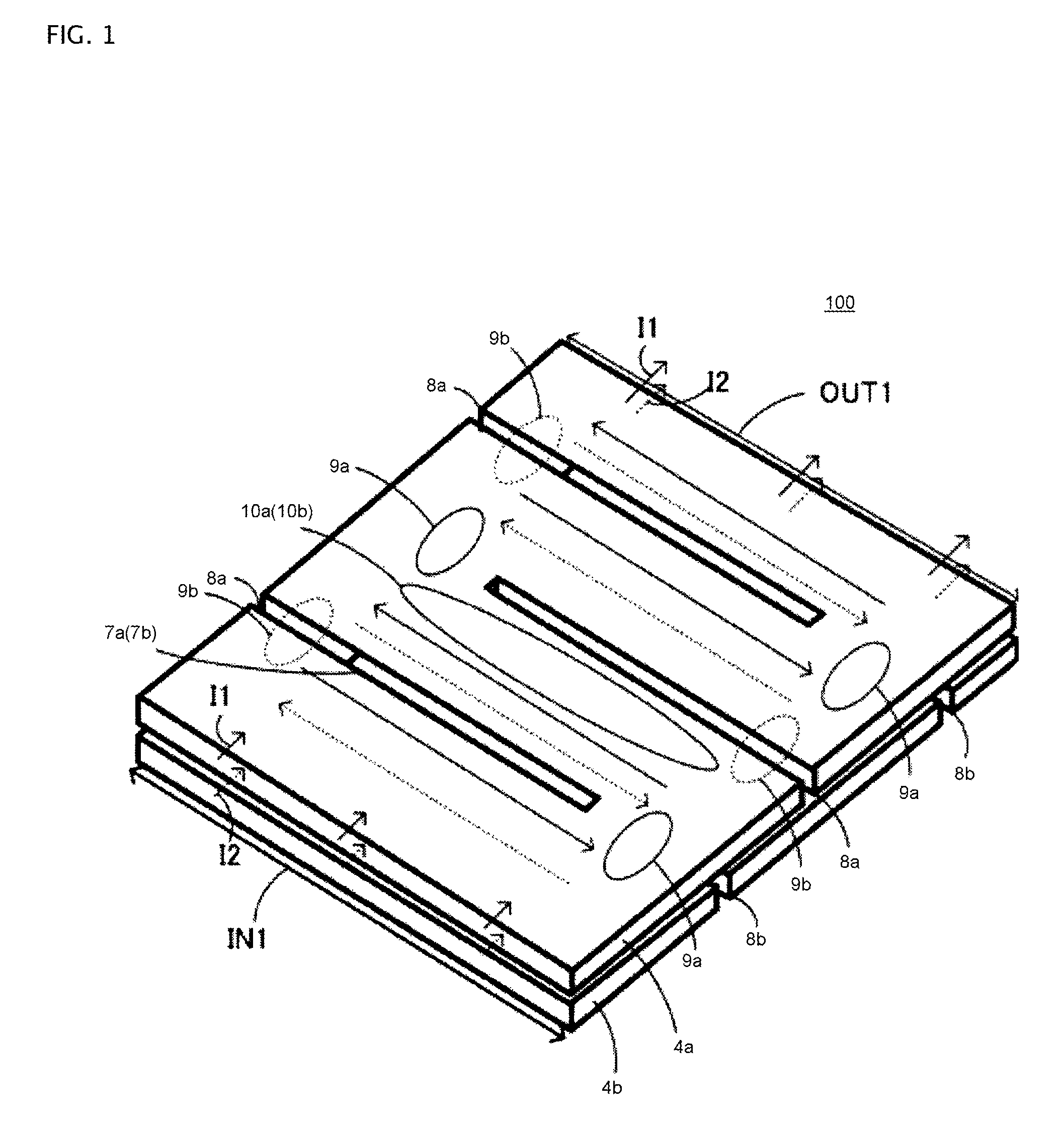
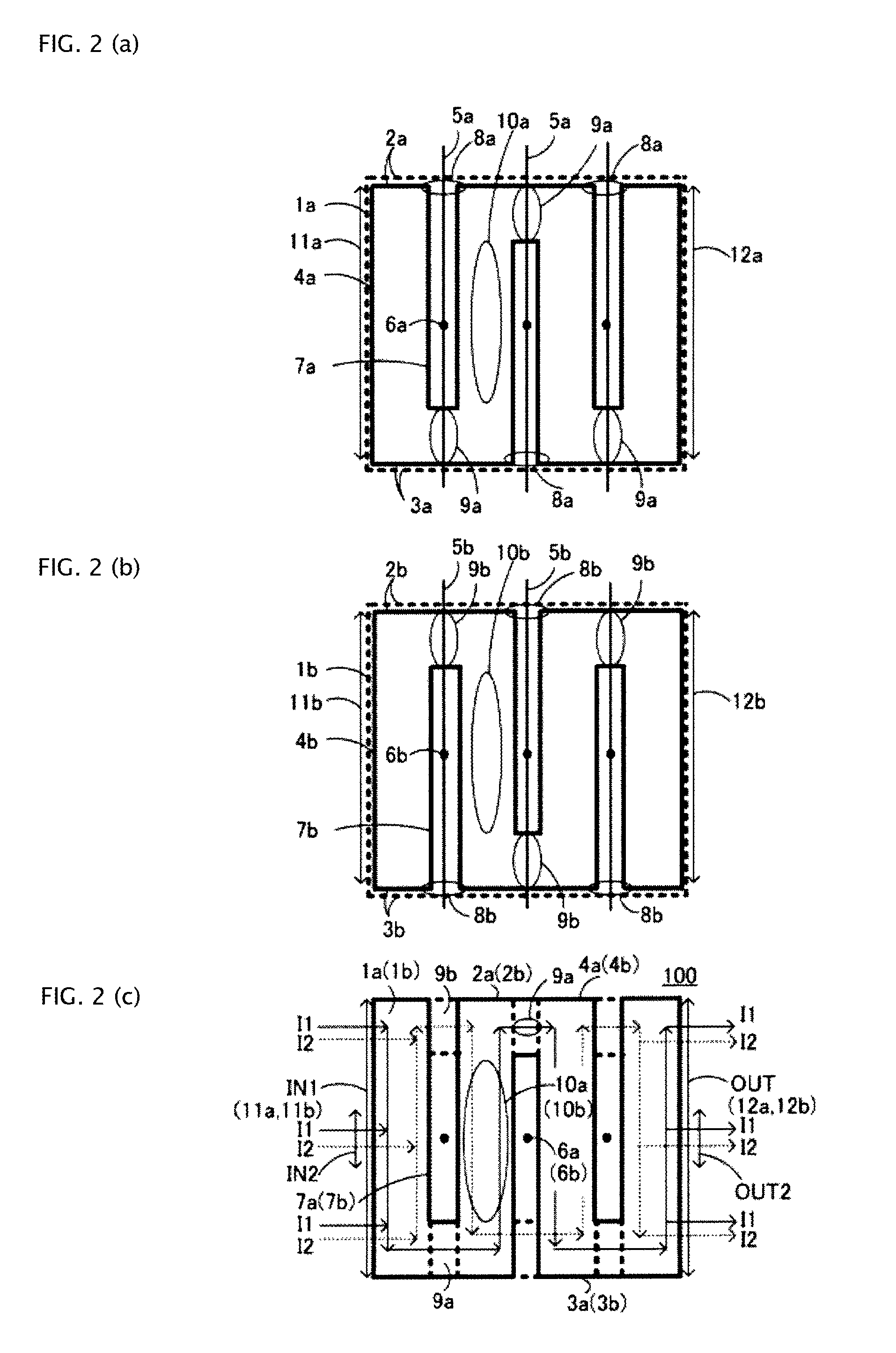
[0041]FIGS. 1 and 2(a)-2(c) are each a substantial configuration diagram of an internal wiring structure of a power semiconductor device according to a first example of the present invention. FIG. 1 is a substantial perspective view. FIG. 2(a) is a substantial plan view of a first wiring conductor. FIG. 2(b) is a substantial plan view of a second wiring conductor. FIG. 2(c) is a substantial plan view in which the first wiring conductor and the second wiring conductor are stacked vertically so as to oppose each other and in parallel to each other. The first wiring conductor 4a and the second wiring conductor 4b correspond to the first wiring conductor 56a and the second wiring conductor 56b shown in FIG. 9, respectively. The two wiring conductors 4a, 4b are stacked so as to oppose each other and in parallel to each other. Currents flow into input parts 11a, 11b of the wiring conductors 4a, 4b in the same direction. Currents flow out of output parts 12a, 12b of the wiring conductors 4...
example 2
[0051]FIGS. 3(a) and 3(b) are a configuration diagram showing an internal wiring structure of a power semiconductor device according to a second example of the present invention. In the diagram, FIG. 3(a) is a substantial plan view, and FIG. 3(b) is a substantial perspective view. The difference between the internal wiring structure of this power semiconductor device 200 and the internal wiring structure of the power semiconductor device 100 shown in FIG. 1 is that the input part IN1 and the output part OUT1 are narrowed to an input part IN2 and an output part OUT2 at the center. This configuration is described hereinafter in detail.
[0052]The corners of the first flat plate 1a and the second flat plate 1b shown in FIG. 1 are cut off to narrow the input part IN1 and the output part OUT1 to the center to obtain the input part IN2 and the output part OUT2 shown in FIGS. 3(a) and 3(b). By forming the input part IN2 and the output part OUT2, the mutual inductance M can be made lower in t...
example 3
[0065]FIGS. 6(a) and 6(b) are a configuration diagram showing an internal wiring structure of a power semiconductor device according to a third example of the present invention. FIG. 6(a) is a substantial plan view, and FIG. 6(b) is a substantial cross-sectional view taken along line X-X of FIG. 6(a). In this example, an internal wiring structure of a power semiconductor module is illustrated as the internal wiring structure of the power semiconductor device.
[0066]FIGS. 7(a) and 7(b) are a configuration diagram of a wiring conductor of FIGS. 6(a) and 6(b). FIG. 7(a) is a substantial plan view of a first wiring conductor 76a, and FIG. 7(b) a substantial plan view of a second wiring conductor 77a. The difference between the power semiconductor device 200 and a power semiconductor module 600 of FIG. 10 is that the wiring conductors 76, 77 are changed to the first and second wiring conductors 76a, 77a. Note that the same reference numerals are used on the sections same as those of the c...
PUM
 Abstract
Description
Claims
Application Information