
Method and apparatus providing wave division multiplexing optical communication system with active carrier hopping

a technology of optical communication system and active carrier, applied in the field of wave division multiplexing optical communication system, can solve problems such as data transmission error potential and signal-to-noise ratio reduction

Active Publication Date: 2014-05-06
MICRON TECH INC
View PDF15 Cites 3 Cited by
  • Summary
  • Abstract
  • Description
  • Claims
  • Application Information

AI Technical Summary

Benefits of technology

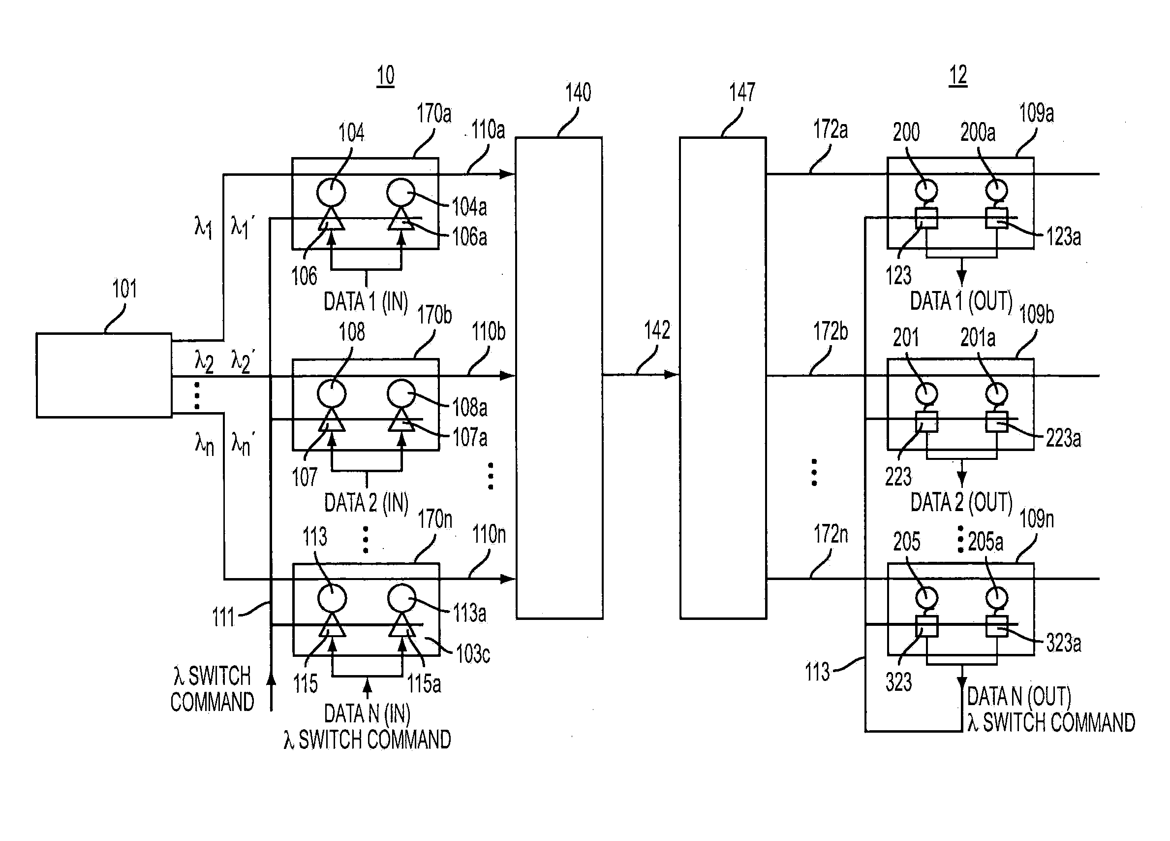
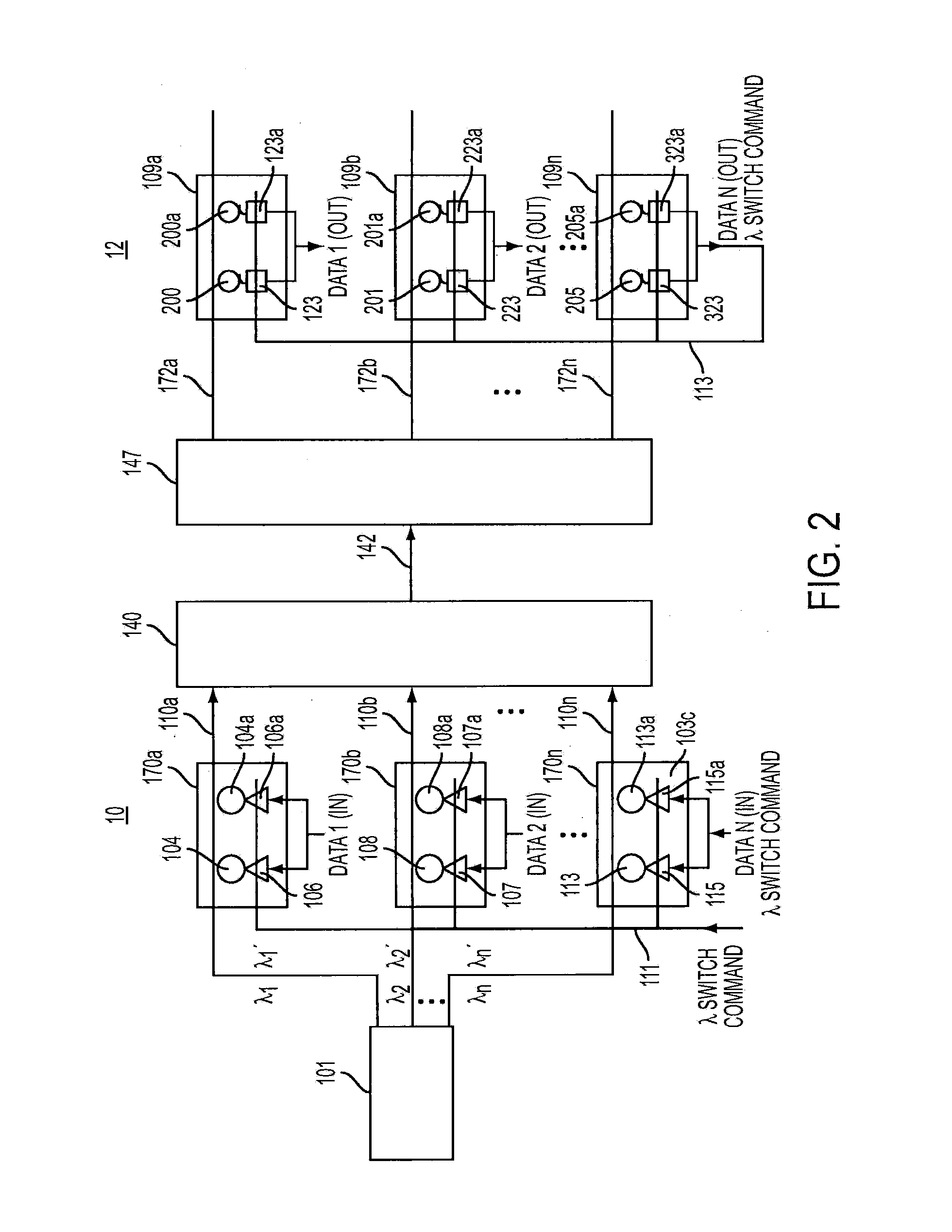
[0016]Example embodiments described herein provide a wave division multiplex (WDM) optical communication system having a plurality of optical communications channels which can be multiplexed and demultiplexed. The WDM optical communications system can be partially or entirely integrated onto a die. Each optical communication channel has at least two spaced carriers and a data modulator having at least a first and a second resonant optical modulator circuit, each associated with a respective carrier. The first resonant optical modulator circuit has a resonant frequency at its respective carrier wavelength and the second resonant modulator circuit has a resonant frequency which is offset from its respective carrier wavelength. When temperature or other changes cause the resonance of the first resonant modulator circuit to move in a direction out of resonance with its associated carrier wavelength the same temperature or other change will also cause the resonant frequency of the second modulator circuit to move in a direction towards resonance with its associated carrier wavelength. A detector which detects when the first modulator circuit is sufficiently out of resonance with its respective carrier wavelength and the second modulator circuit is in sufficient resonance with its respective carrier wavelength is used to control switching of data modulation from the first to the second modulator circuit. As a consequence, data for a given optical communication channel is switched to a different channel carrier wavelength where it is reliably modulated by the second modulator circuit.

Problems solved by technology

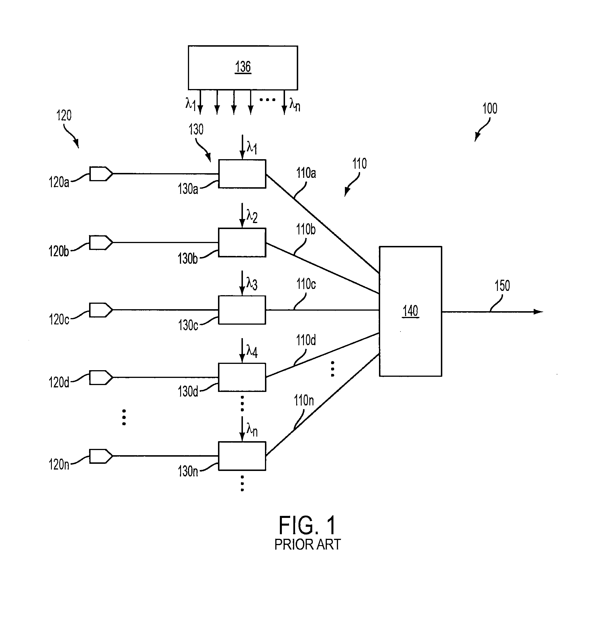
. . 130n drops resulting in reduced signal-to-noise ratio and the potential for data transmission errors.

Method used


Image

  • Method and apparatus providing wave division multiplexing optical communication system with active carrier hopping
  • Method and apparatus providing wave division multiplexing optical communication system with active carrier hopping
  • Method and apparatus providing wave division multiplexing optical communication system with active carrier hopping

Examples


Embodiment Construction

[0016]Example embodiments described herein provide a wave division multiplex (WDM) optical communication system having a plurality of optical communications channels which can be multiplexed and demultiplexed. The WDM optical communications system can be partially or entirely integrated onto a die. Each optical communication channel has at least two spaced carriers and a data modulator having at least a first and a second resonant optical modulator circuit, each associated with a respective carrier. The first resonant optical modulator circuit has a resonant frequency at its respective carrier wavelength and the second resonant modulator circuit has a resonant frequency which is offset from its respective carrier wavelength. When temperature or other changes cause the resonance of the first resonant modulator circuit to move in a direction out of resonance with its associated carrier wavelength the same temperature or other change will also cause the resonant frequency of the second...


PUM


Abstract

A wave division multiplexing (WDM) system is disclosed which accommodates shifts in the resonant frequency of optical modulators by using at least two carriers per optical communications channel and at least two resonant modulator circuits respectively associated with the carriers within each optical modulator. A first resonant modulator circuit resonates with a first carrier and a second resonates with a second carrier when there is a shift in resonance frequency of the at least two resonant optical modulator circuits. A switch circuit controls which carrier is being modulated by its respective resonant modulator circuit.

Description

FIELD OF THE INVENTION[0001]Embodiments of the present invention relate to wave division multiplexing optical communication systems which compensate for operational changes in photonic devices due to temperature changes.BACKGROUND OF THE INVENTION[0002]Silicon-based integrated circuits have long been used as a platform for microelectronic applications. More recently, as speed, bandwidth and signal processing requirements have increased, optical systems are now also being integrated on silicon-based integrated circuits.[0003]Thus, instead of or in addition to using silicon to facilitate the flow of electricity, silicon is used to direct the flow of light. While the speed of electricity and the speed of light are the same, light is able to carry more data over a given optical path than can electricity over a given electrical path. Accordingly, there are significant advantages to using light as a data carrier. Furthermore, using silicon as the optical medium allows for application of, ...

Claims


Application Information

Patent Timeline
Patent Type & Authority Patents(United States)
IPC IPC(8): H04J14/02H04B10/032
CPCH04J14/02H04B10/506H04Q11/0005
Inventor MEADE, ROYSANDHU, GURTEJ
Owner MICRON TECH INC
Learn More