Signal modulation circuit

a signal modulation circuit and signal technology, applied in the field of signal modulation circuits, can solve problems such as noise shaping, and achieve the effect of reliably modulating and reducing the influence of distortion/noise components in the delay devi

Active Publication Date: 2016-05-24
ONKYO KK
View PDF14 Cites 0 Cited by
  • Summary
  • Abstract
  • Description
  • Claims
  • Application Information

AI Technical Summary

Benefits of technology

[0009]It is an object of the present invention to provide a circuit that can correct an output state in real time, can reduce an influence of distortion / noise components in a delay device, and can reliably modulate an input signal so as to output the modulated signal.
[0011]In the present invention, unlike the conventional delta sigma modulation circuit, a delay circuit is not provided to a feedback circuit for negatively feeding back an output signal of the quantizer, but a delay function is provided between the integrator and the quantizer. Thus, the output state can be corrected in real time. A zero level (zero voltage) is inserted into a signal integrated by the integrator at timing synchronized with a clock signal, so that pulse density modulation (PDM) can be reliably performed on an input signal.
[0019]According to the present invention, an output state can be corrected in real time, and an influence of distortion / noise components in the delay device can be reduced, and an input signal can be reliably modulated so as to be output. In addition, according to the present invention, a ternary signal of +1, 0, and −1 can be generated. Further, according to the present invention, the loudspeaker connected to the single power supply can be driven in a ternary state.

Problems solved by technology

At the same time, however, the configuration has a problem that the delay device 12 in the feedback path cannot correct an output state in real time, or a problem that noise shaping is not performed on distortion / noise components generated in the delay device and the distortion / noise components are directly output.

Method used


Image

  • Signal modulation circuit
  • Signal modulation circuit
  • Signal modulation circuit

Examples


first embodiment

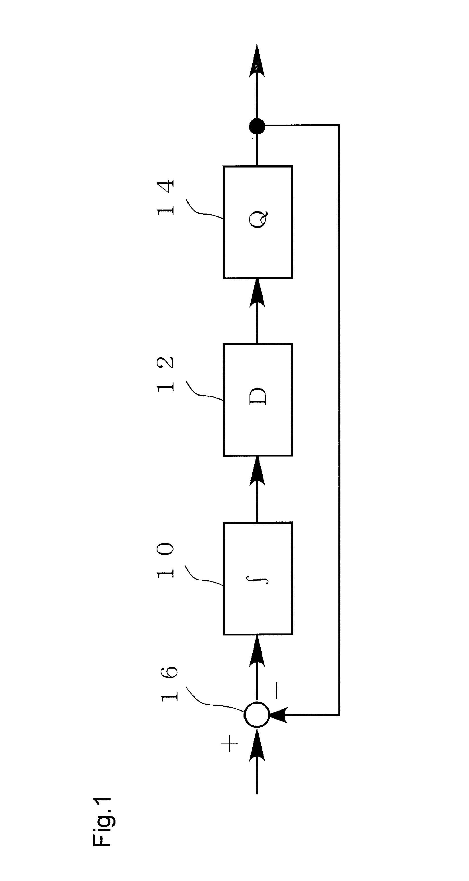
[0039]FIG. 1 illustrates a basic configuration of a signal modulation circuit according to the first embodiment. The signal modulation circuit according to this embodiment performs delta sigma modulation on an input signal, and includes a subtracter 16, an integrator 10, a delay device 12, and a quantizer 14.

[0040]The circuit shown in FIG. 1 is compared with a circuit shown in FIG. 17. In the circuit according to this embodiment, the delay device 12 is not present on a feedback path, but is provided at a front stage of the quantizer 14, that is, between the integrator 10 and the quantizer 14. Therefore, in the circuit according to this embodiment, an output state can be corrected in real time.

[0041]The delay device 12 according to this embodiment has a function for not only delaying an input signal but also inserting a zero level into an input signal, and this realizes more reliable pulse density modulation. Any circuit for inserting the zero level into an input signal is used, but ...

second embodiment

[0059]The spread of portable devices and the demand for energy saving in recent years require further promotion of efficiency of class-D amplifiers. Since general class-D amplifiers express a level using an average value of two signals of a positive voltage and a negative voltage, as to a non-signal state that is a zero voltage, a positive voltage and a negative voltage are expressed by a duty of 50%. That is, in the class-D amplifiers realized by binary signals, switching cross occurs also at the non-signal time, and thus the improvement in the switching cross is demanded. However, it is difficult for a binary signal to generate a state where switching is not performed at the non-signal state.

[0060]The second embodiment, therefore, describes a configuration in which, while the configuration in the first embodiment is being used, a ternary PDM signal of +1, 0, and −1 are generated so that the state where the switching is not performed at the non-signal time is generated.

[0061]FIG. 6...

third embodiment

[0073]In the second embodiment, a ternary PDM signal of +1, 0, and −1 is generated to be output, and the bias generating circuit 30 and the bias generating circuit 31 apply a bias voltage so that the switching at the non-signal time is suppressed. However, since a bias voltage is applied not only at the non-signal time but also at a signal generated time, distortion may occur.

[0074]The third embodiment, therefore, describes a circuit configuration in which the switching at the non-signal time is suppressed, and distortion at the signal generated time can be reduced.

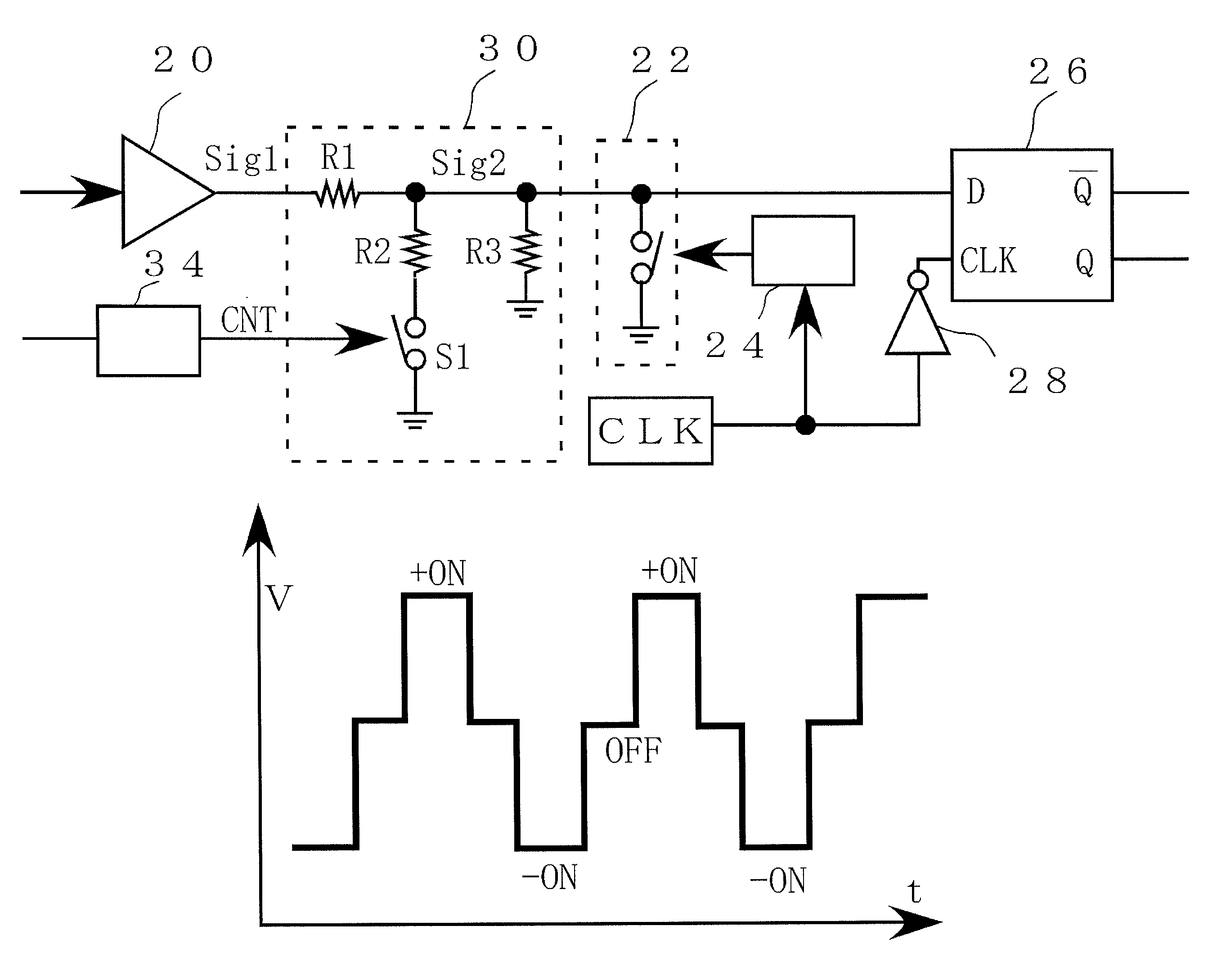
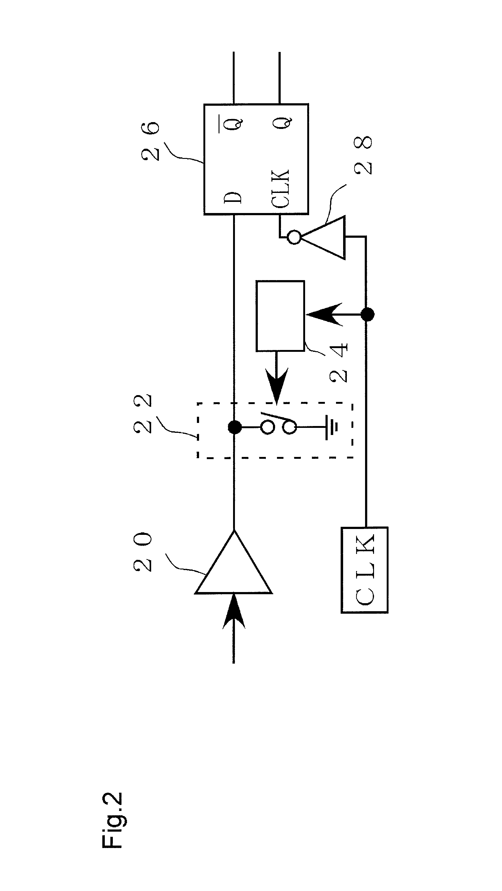
[0075]FIG. 10 illustrates a circuit configuration according to this embodiment. In addition to the circuit configuration shown in FIG. 6, a signal detector 34 is further provided. In FIG. 10, in view of the matching of the configuration between the bias generating circuit 30 and the bias generating circuit 31, the configuration is illustrated for both the circuits.

[0076]The signal detector 34 detects presence and absence ...


PUM

PropertyMeasurementUnit
phaseaaaaaaaaaa
bias voltageaaaaaaaaaa
bias voltagesaaaaaaaaaa

Abstract

Provided is a modulation circuit that can correct an output state in real time and reliably modulate an input signal to output the modulated signal. The signal modulation circuit includes a subtracter, an integrator, a chopper circuit, a frequency divider, and a D-type flip-flop. A delay circuit of a sigma delta modulation circuit is not provided to a feedback circuit, and a signal is delayed and quantized in the D-type flip-flop. The chopper circuit inserts a zero level at timing synchronized with a clock signal, so that pulse density modulation is performed.

Description

BACKGROUND OF THE INVENTION[0001]1. Field of the Invention[0002]The present invention relates to a signal modulation circuit, and particularly relates to a circuit for performing delta sigma modulation.[0003]2. Description of the Related Art[0004]Conventionally, delta sigma modulation (ΔΣ modulation) is used in switching amplifiers or the like. A delta sigma modulator has a subtracter, an integrator, a quantizer, and a quantization error feedback circuit.[0005]FIG. 17 illustrates a basic configuration of a delta sigma modulation circuit. A subtracter 16 calculates a difference between an input signal and a feedback signal, and an integrator 10 integrates the difference signal. An integral signal is quantized by a quantizer 14 and is output as, for example, 1 bit (=binary) signal. The quantization error is fed back via a delay device 12.[0006]JP 2007-312258 A discloses a delta sigma modulation circuit including an integrator group, an adder group, a quantizer, and a pulse width round...

Claims


Application Information

Patent Timeline
Patent Type & Authority Patents(United States)
IPC IPC(8): H03M3/00G11B20/10G11B20/00H04R3/00
CPCH03M3/30G11B20/10009H03M3/346H03M3/348H04R3/00G11B2020/00065H03M3/37H03M3/424
Inventor NAKANISHI, YOSHINORIKAWAGUCHI, TSUYOSHISEKIYA, MAMORU
Owner ONKYO KK
Why Eureka
Try Eureka