Lead-frame circuit package

a technology of lead frame and circuit, applied in the direction of electrical apparatus, semiconductor devices, semiconductor/solid-state device details, etc., can solve the problems of loss of power gain, need to dissipate energy, increase the difficulty of miniaturization of the package, etc., and achieve the effect of low cost structure and worse grounding

Active Publication Date: 2014-05-27
NXP USA INC
View PDF11 Cites 4 Cited by
  • Summary
  • Abstract
  • Description
  • Claims
  • Application Information

AI Technical Summary

Problems solved by technology

The substantially high transmission power associated with RF communication (for example class 12 global system for mobile communication (GSM) or general packet radio system (GPRS) communication) where the transmit time is half of the total communication time, forces the need to dissipate the energy in a restricted area and increases the difficulty of miniaturization of the package.
This leads to a loss of power gain, which is highly undesirable.
Furthermore, due to space constraints in being able to build an RF module using such lead-frame technology, the only other component on the die is the power amplifiers' associated control functionality 115.
It is known that it is very difficult to implement high-Q inductors in a small size and at a low cost, as shown by the inductive tracks 120 implemented on the lead-frame package.
Furthermore, implementing discrete inductors is impractical, due to the size and cost of such components.
Unfortunately, the aforementioned use of high-Q lead-frame inductors 120 proposed in U.S. Pat. No. 6,621,140 B1 occupies about 40% of the PA area, thereby removing any practical possibility to implement a complete front-end module.
Furthermore, due to the extensive use of inductive tracks that are required to manufacture a complete RF front-end module, a lead-frame package provides poor signal routeing capability.
However, it is noteworthy that none of the above citations adequately address the aforementioned problem of implementing a RF power module having an improved power performance.
In particular, none of the above citations disclose a mechanism that improves power added efficiency, where sufficiently less die size is required to implementing high-Q components, such as inductors, capacitors and RF chokes.
It is also well known that a resistive or inductive grounding of the RF power device generates fast degradation of power gain and power added efficiency.
A primary weakness of this structure is a significantly worse grounding, as compared to the RF die grounding of soldering directly on a metallic flange as shown in FIG. 2.

Method used


Image

  • Lead-frame circuit package
  • Lead-frame circuit package
  • Lead-frame circuit package

Examples


Embodiment Construction

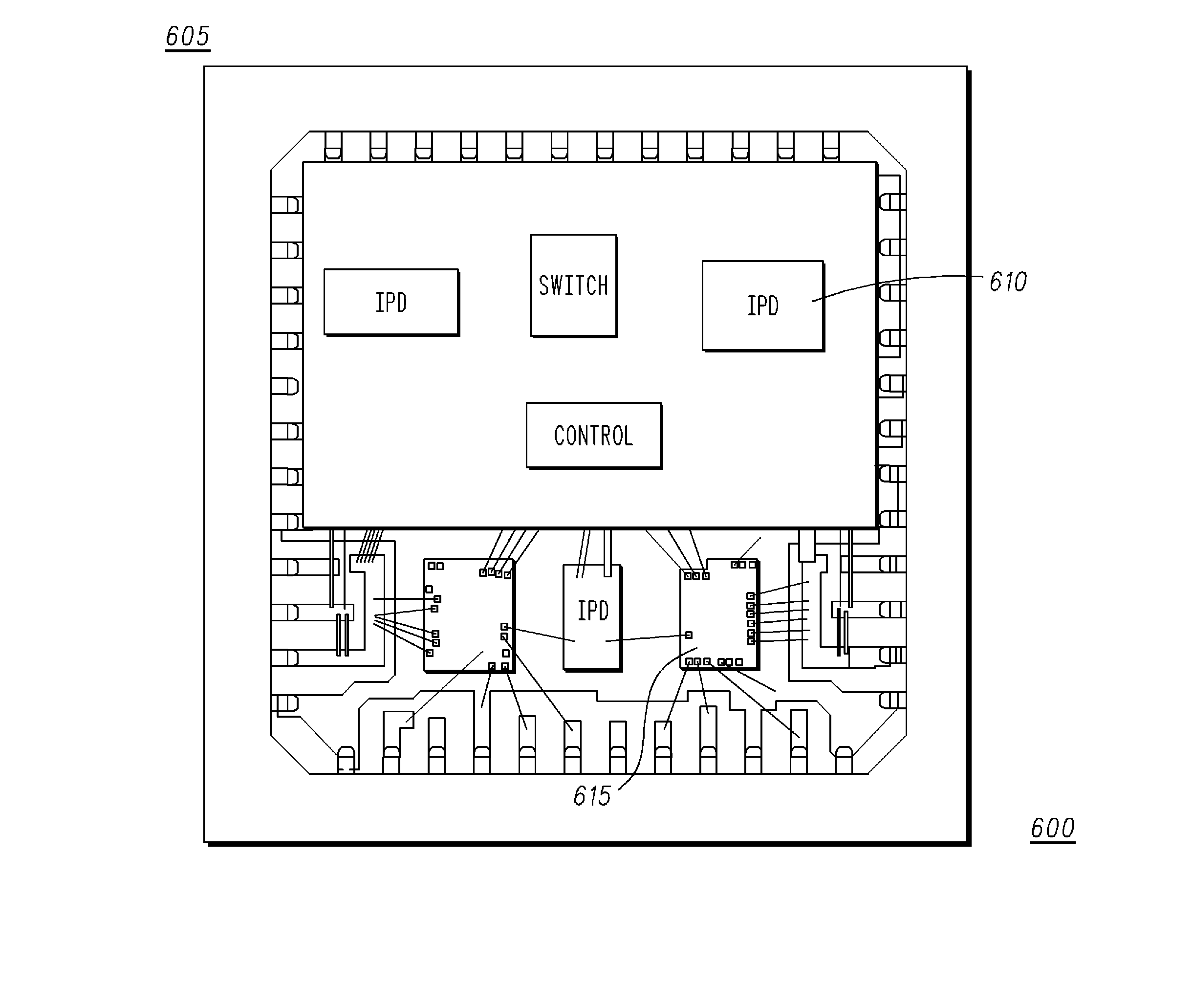
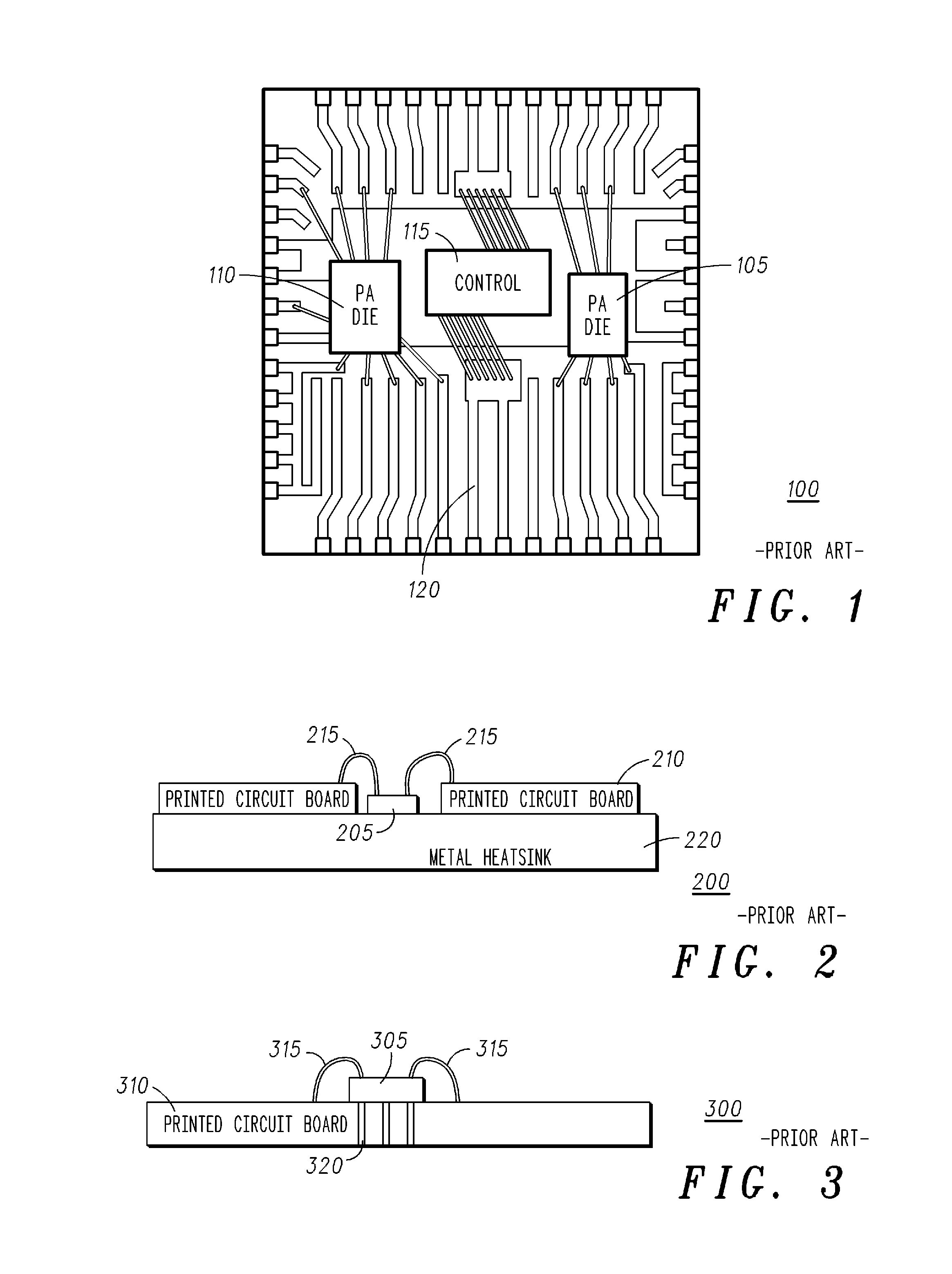
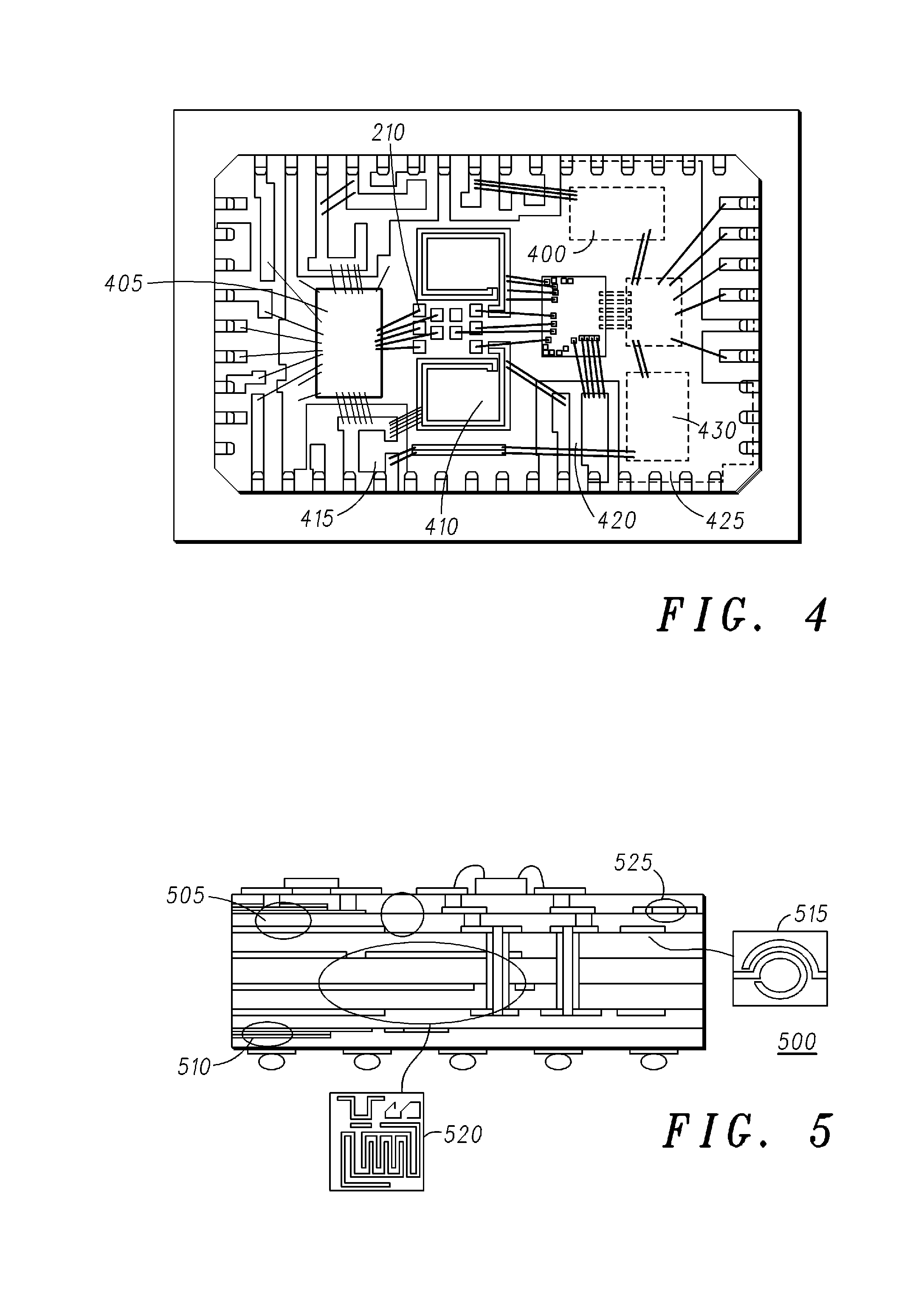
[0039]The preferred embodiment of the present invention will be described in terms of a lead-frame package for a radio frequency (RF) power amplifier (PA) module capable of operation in digital wireless cellular communication units, such as GSM, Edge, or 3rd generation (3G) cellular phones. However, it will be appreciated that the inventive concepts herein described may be embodied in any radio frequency amplifier device or apparatus.

[0040]In the context of the present invention, the term ‘lead-frame packaging’ encompasses, at least, any metal frame that provides external electrical connection to a packaged integrated circuit (IC) or chip, as they are commonly referred to.

[0041]Furthermore, in the context of the present invention, the term ‘substrate’ encompasses, at least, any organic or ceramic printed circuit board (PCB) that provides internal (die to die and / or die to surface mount technology (SMT) components) and external electrical connection to the packaged chip.

[0042]It is a...


PUM


Abstract

A lead-frame circuit package comprises a die and a substrate located thereon to route radio frequency signals to / from the die. The package preferably comprises an exposed pad on the die to receive a power amplifier device wherein the substrate is used to provide high-Q elements such as RF chokes on signal paths to / from the power amplifier device.In this manner, the design benefits from the power capabilities and improved grounding of a lead-frame conductor, whilst also achieving the routeing capabilities and small scale advantages provided by a multi-layer printed circuit substrate.

Description

FIELD OF THE INVENTION[0001]The preferred embodiment of the present invention relates to a lead-frame circuit package. The invention is applicable to, but not limited to, a lead-frame circuit package suitable for use with a radio frequency power amplifier module or a front-end module.BACKGROUND OF THE INVENTION[0002]The present invention relates to radio frequency (RF) power amplifier (PA) and front-end modules (FEM). Typical applications targeted for such technologies are cellular phones, Personal Digital assistants (PDA) and wireless connectivity applications such as Digital video Broadcast (DVB-H and DVB-T), Zigbee, wireless local area networks (WLAN) and Ultra wideband applications (UWB). The substantially high transmission power associated with RF communication (for example class 12 global system for mobile communication (GSM) or general packet radio system (GPRS) communication) where the transmit time is half of the total communication time, forces the need to dissipate the en...

Claims


Application Information

Patent Timeline
Patent Type & Authority Patents(United States)
IPC IPC(8): H01L23/495
CPCH01L2924/30107H01L2924/1433H01L23/49531H01L23/64H01L2224/48137H01L2224/32245H01L2924/01075H01L2924/10329H01L2224/16H01L2924/01082H01L2924/1517H01L2224/48247H01L2924/0106H01L2924/0001H01L2924/01027H01L2224/48091H01L23/49575H01L2924/01033H01L24/45H01L2924/15153H01L2224/29111H01L2924/01079H01L2223/6644H01L2924/01083H01L2224/45144H01L2924/01322H01L2924/01013H01L2924/014H01L2924/14H01L2224/49171H01L24/48H01L24/29H01L2924/01014H01L2224/73265H01L2924/01023H01L2924/0105H01L2924/15747H01L24/49H01L2924/01032H01L2924/3011H01L2924/19041H01L2924/01031H01L2924/0132H01L2924/01029H01L2924/09701H01L2224/16245H01L2924/15787H01L2924/30111H01L2924/181H01L2924/12042H01L24/73H01L2924/00014H01L2924/00H01L2924/00012H01L2224/29099
Inventor MONTORIOL, JR., GILLESDELAUNAY, THIERRYTILHAC, FREDERIC
Owner NXP USA INC
Why Eureka
Try Eureka