Transistors, semiconductor memory cells having a transistor and methods of forming the same

a technology of semiconductor memory cells and transistors, which is applied in the direction of transistors, semiconductor devices, electrical devices, etc., can solve the problems of difficult to increase limited information storage elements, etc., and achieve the effect of increasing the data sensing margin of the semiconductor device and large data storage capacity

Active Publication Date: 2014-07-08
SAMSUNG ELECTRONICS CO LTD
View PDF20 Cites 2 Cited by
  • Summary
  • Abstract
  • Description
  • Claims
  • Application Information

AI Technical Summary

Benefits of technology

[0007]Example embodiments provide a transistor having a larger data storage capacity such that a data sensing margin of a semiconductor device is increased and a method of forming the transistor.
[0008]Example embodiments also provide a semiconductor memory cell, which prevents information storage elements corresponding to adjacent transistors from inverting data during the drive of a semiconductor device.

Problems solved by technology

As such, the information storage element may be limited to the size of the gate pattern.
Because the information storage element, which may be limited in size, corresponds to a portion of the semiconductor substrate that provides a bipolar operation, it may be difficult to increase a data sensing margin of the semiconductor device.

Method used


Image

  • Transistors, semiconductor memory cells having a transistor and methods of forming the same
  • Transistors, semiconductor memory cells having a transistor and methods of forming the same
  • Transistors, semiconductor memory cells having a transistor and methods of forming the same

Examples


Embodiment Construction

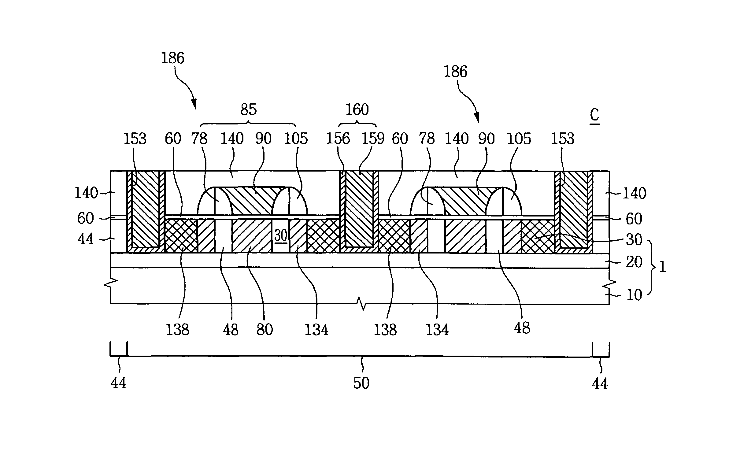
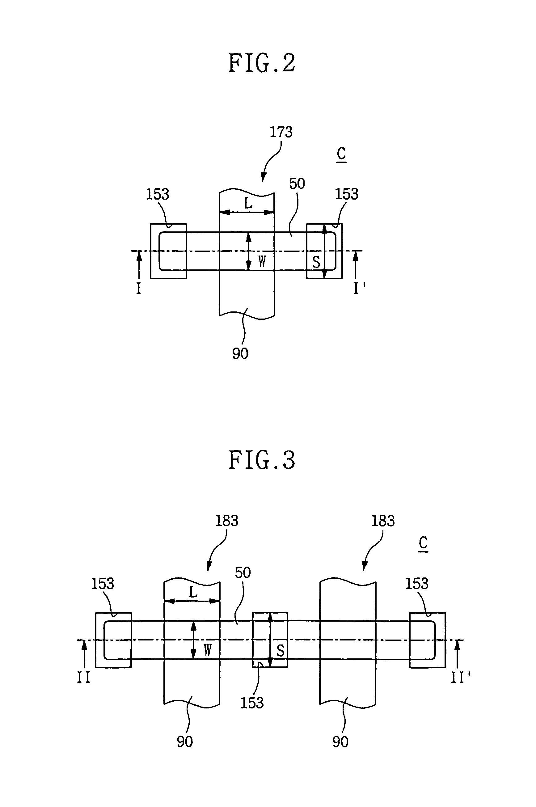
[0042]Various example embodiments will now be described more fully with reference to the accompanying drawings in which some example embodiments are shown. However, specific structural and functional details disclosed herein are merely representative for purposes of describing example embodiments. Thus, the invention may be embodied in many alternate forms and should not be construed as limited to only example embodiments set forth herein. Therefore, it should be understood that there is no intent to limit example embodiments to the particular forms disclosed, but on the contrary, example embodiments are to cover all modifications, equivalents, and alternatives falling within the scope of the invention.

[0043]In the drawings, the thicknesses of layers and regions may be exaggerated for clarity, and like numbers refer to like elements throughout the description of the figures.

[0044]Although the terms first, second, etc. may be used herein to describe various elements, these elements s...


PUM


Abstract

Transistors, semiconductor memory cells having a transistor and methods of forming the same are provided, the transistors may include a semiconductor substrate having a first semiconductor region. A gate pattern may be disposed on the first semiconductor region. Spacer patterns may each be disposed on a sidewall of the gate pattern. Second semiconductor regions and a third semiconductor regions may be disposed in the semiconductor substrate. The second semiconductor regions may be disposed under the spacer patterns. The third semiconductor regions may be disposed adjacent to the second semiconductor regions. The first semiconductor region may have a higher impurity ion concentration than the second semiconductor regions.

Description

CROSS-REFERENCE TO RELATED APPLICATION[0001]This application claims the benefit under 35 U.S.C. §119 to Korean Patent Application No. 10-2008-0099064, filed on Oct. 9, 2008 with the Korean Intellectual Property Office (KIPO), the entire contents of which are incorporated herein by reference in their entirety.BACKGROUND[0002]1. Field[0003]Example embodiments relate to transistors, semiconductor memory cells having a transistor and methods of forming the same. Other example embodiments relate to transistors having a larger data storage capacity, semiconductor memory cells having the transistors and methods of forming the same.[0004]2. Description of Related Art[0005]In recent years, semiconductor devices are being fabricated wherein a semiconductor memory cell uses only a transistor to enable semiconductor memory operations, without forming an information storage element on a semiconductor substrate. If the information storage element is formed by implanting impurity ions in the semic...

Claims


Application Information

Patent Timeline
Patent Type & Authority Patents(United States)
IPC IPC(8): H01L27/12
CPCH01L29/7841H01L21/28114H01L27/108H01L27/10802H01L27/1203H01L29/41733H01L29/66553H01L29/7843H01L29/7846H10B12/20H10B12/00
Inventor TAK, NAM-KYUNSONG, KI-WHAN
Owner SAMSUNG ELECTRONICS CO LTD
Why Eureka
Try Eureka