Interconnect structure and method of making same

a technology of interconnects and structures, applied in the direction of semiconductor devices, semiconductor/solid-state device details, electrical apparatus, etc., can solve the problems of circuit malfunction, loss of one or more connections, and reducing the reliability of integrated circuits

Active Publication Date: 2014-07-08
GLOBALFOUNDRIES U S INC
View PDF18 Cites 4 Cited by
  • Summary
  • Abstract
  • Description
  • Claims
  • Application Information

AI Technical Summary

Benefits of technology

This patent describes a method for preventing unwanted deposition and nucleation of capping material on a dielectric layer during semiconductor device manufacturing. A sacrificial material is deposited on the dielectric layer and then removed to prevent this deposition. The sacrificial material can be hydrophobic and can be polyxylylene polymers or silylating agents. The method can be carried out using UV assisted thermal composition, thermal decomposition, or reducing plasma etch. This technique helps to improve the quality and reliability of semiconductor devices.

Problems solved by technology

In fact, electromigration is known to decrease the reliability of integrated circuits (ICs) and hence lead to a malfunction of the circuit.
In the worst case, for example, electromigration leads to the eventual loss of one or more connections and intermittent failure of the entire circuit.
This increased current density degrades EM (electromigration) related reliability.
Thus, with increasing miniaturization the probability of failure due to electromigration increases in VLSI and ULSI circuits because both the power density and the current density increase.
Although the selective electroless metal cap deposition process is selective to copper, unwanted deposition and / or rogue nucleation of the CoWP still results on the surface of the interlevel dielectric of the structure.
This, in turn, results in high leakage and poor time dependent dielectric breakdown.
In fact, the unwanted deposition and / or rogue nucleation can cause device failure due to shorting between adjacent copper lines.

Method used


Image

  • Interconnect structure and method of making same
  • Interconnect structure and method of making same
  • Interconnect structure and method of making same

Examples


Embodiment Construction

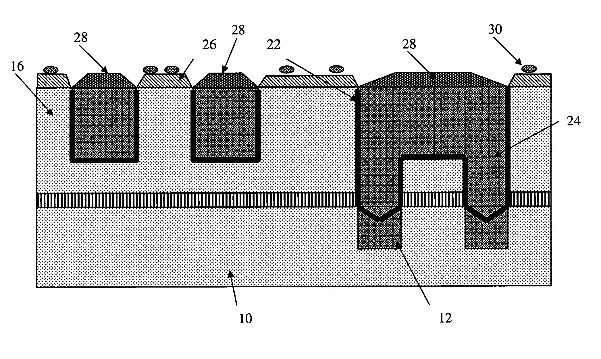
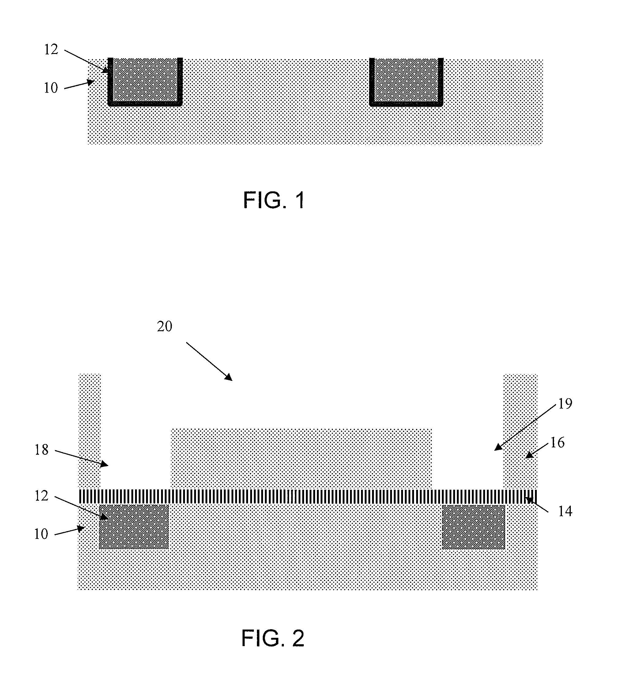
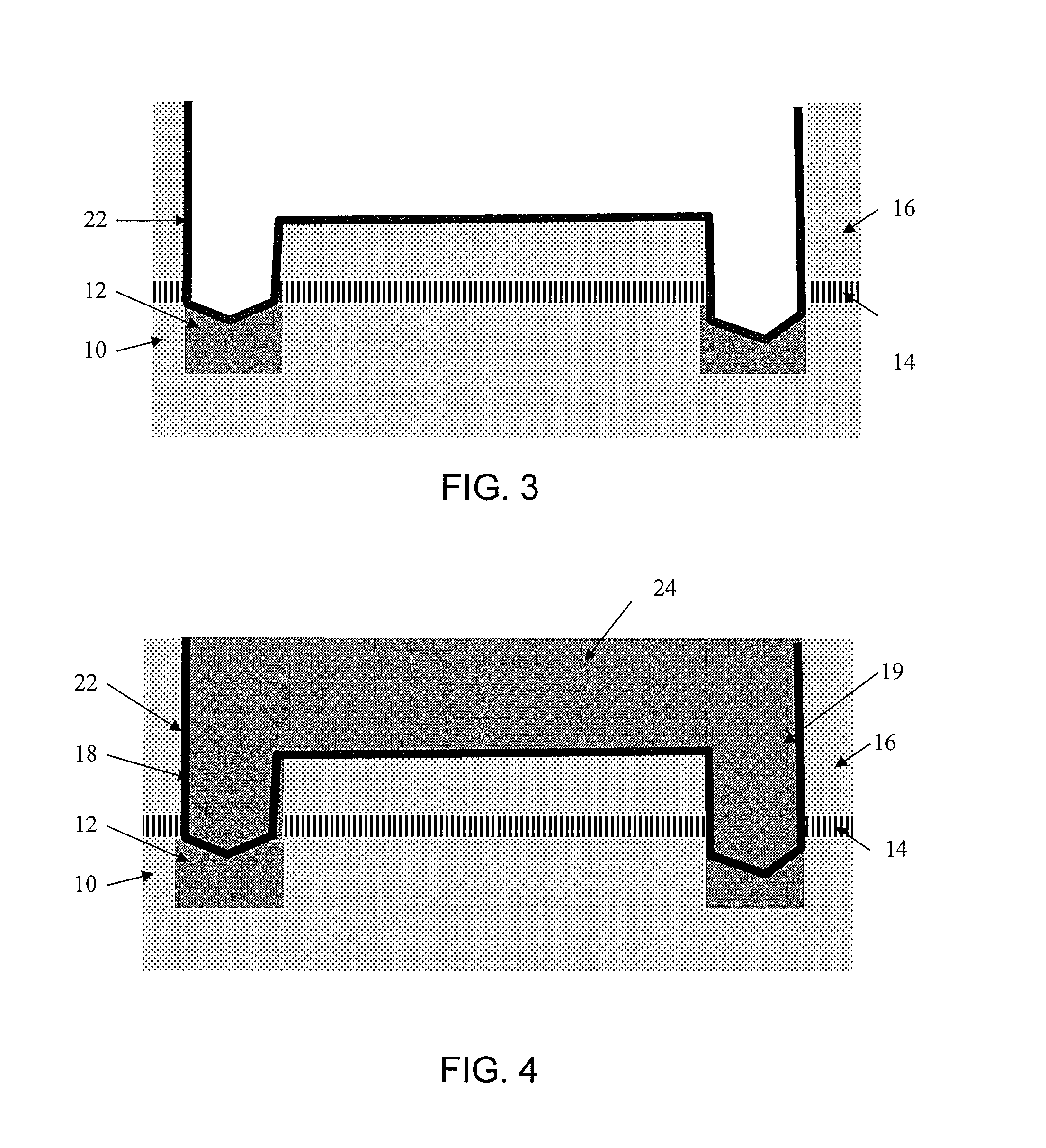
[0022]The present invention relates generally to an interconnect structure and method of fabricating the same and, more particularly, to a defect free capped interconnect structure and method of fabricating the same. By implementing the fabrication processes and structure in accordance with the invention, the copper interconnect is more reliable than conventional structures and hence is not prone to failure due to shorting, e.g., shorting between copper wires as a result of nucleation.

[0023]For example, advantageously, by implementing the fabrication processes and structure in accordance with the invention, the surface of the interlevel dielectric is free of capping material such as, for example, CoWP or CoWB. That is, by implementing the fabrication processes of the invention, the resultant structure is free of unwanted deposition and / or rogue nucleation of the CoWP (or other capping material) on the surface of the interlevel dielectric. This, in turn, results in low leakage and in...


PUM

PropertyMeasurementUnit
temperaturesaaaaaaaaaa
direct current densitiesaaaaaaaaaa
current densityaaaaaaaaaa

Abstract

An interconnect structure and method of fabricating the same is provided. More specifically, the interconnect structure is a defect free capped interconnect structure. The structure includes a conductive material formed in a trench of a planarized dielectric layer which is devoid of cap material. The structure further includes the cap material formed on the conductive material to prevent migration. The method of forming a structure includes selectively depositing a sacrificial material over a dielectric material and providing a metal capping layer over a conductive layer within a trench of the dielectric material. The method further includes removing the sacrificial material with any unwanted deposited or nucleated metal capping layer thereon.

Description

FIELD OF THE INVENTION[0001]The present invention relates generally to an interconnect structure and method of fabricating the same and, more particularly, to a defect free capped interconnect structure and method of fabricating the same.BACKGROUND OF THE INVENTION[0002]Electromigration is the transport of material caused by the gradual movement of ions in a conductor due to the momentum transfer between conducting electrons and diffusing metal atoms. The effect of electromigration is an important consideration to take into account in applications where high direct current densities are used, such as in microelectronics and related structures. In fact, electromigration is known to decrease the reliability of integrated circuits (ICs) and hence lead to a malfunction of the circuit. In the worst case, for example, electromigration leads to the eventual loss of one or more connections and intermittent failure of the entire circuit.[0003]The current density in interconnect structures in...

Claims


Application Information

Patent Timeline
Patent Type & Authority Patents(United States)
IPC IPC(8): H01L23/48
CPCH01L23/53238H01L23/5226H01L23/53204H01L21/76829H01L21/76805H01L23/53295H01L21/76849C23F4/00H01L2924/0002H01L2924/00
Inventor OU, YAPONOTH, SHOMSPOONER, TERRY A.
Owner GLOBALFOUNDRIES U S INC
Why Eureka
Try Eureka