

Semiconductor device fabricating method and system for carrying out the same
a semiconductor device and fabricating method technology, applied in the direction of coatings, metallic material coating processes, chemical vapor deposition coatings, etc., can solve the problems of reducing breakdown voltage, increasing leakage current that leaks from transistors or reducing breakdown voltage, and titanium nitride film only has limited grain sizes
- Summary
- Abstract
- Description
- Claims
- Application Information
AI Technical Summary
Benefits of technology
Problems solved by technology
Method used
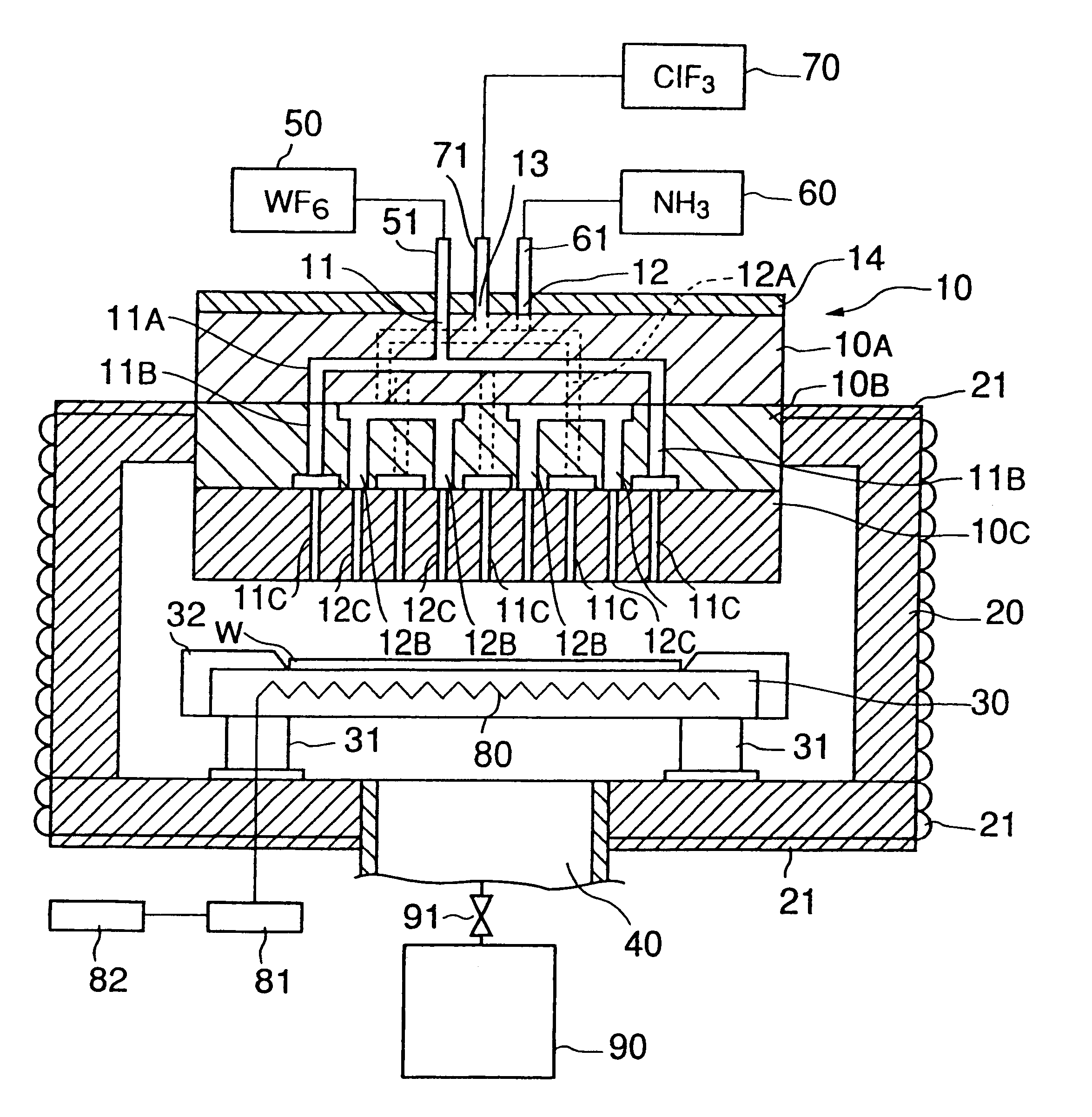
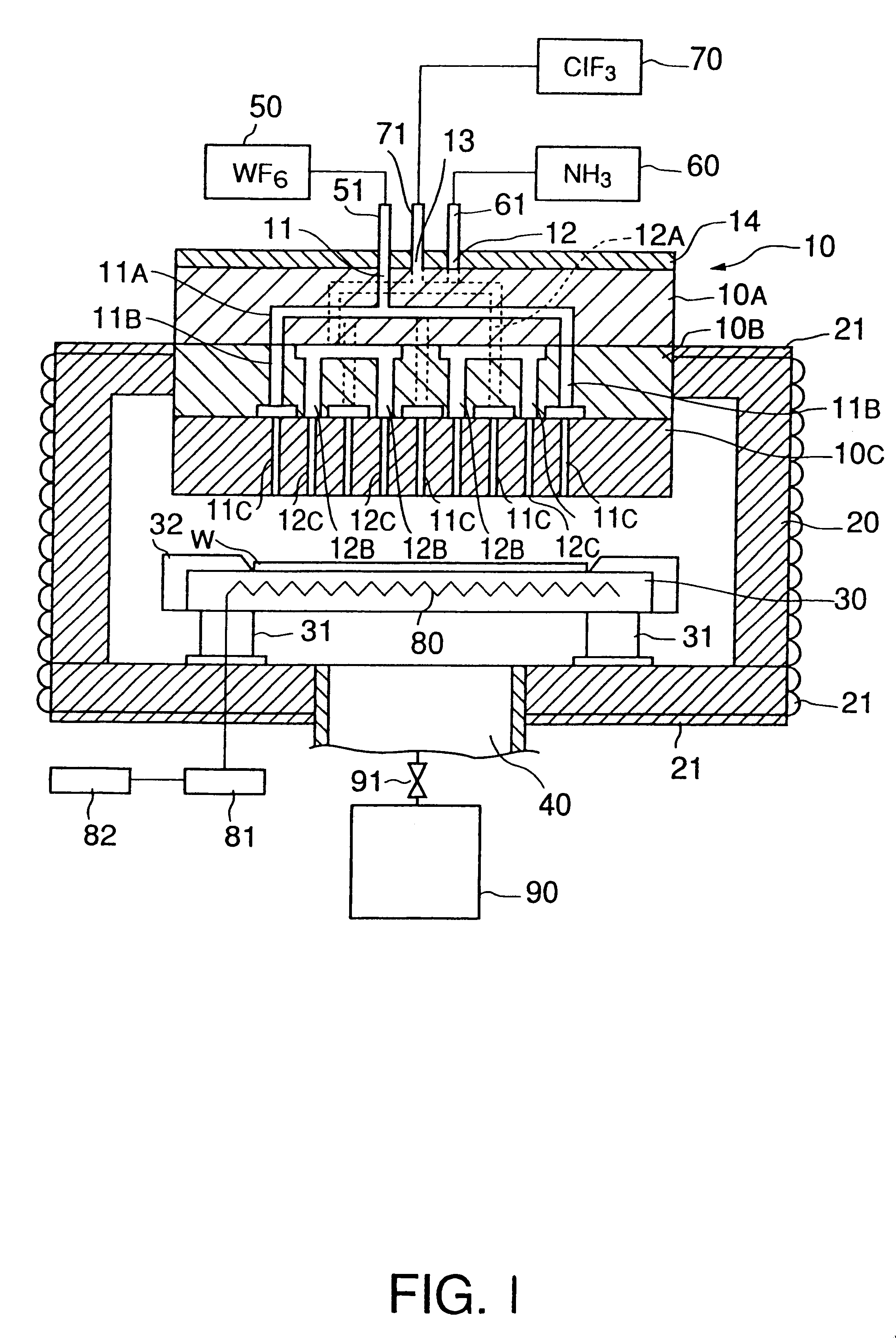
Image

Examples
example 2
A semiconductor device fabricating method in Example 2 formed a W / WN.sub.x / poly-Si film on a semiconductor wafer having a poly-Si film on its surface by the same process conditions as those for Example 1. Subsequently, a WN.sub.x / W / WN.sub.x / poly-Si film was formed by forming a WN.sub.x film on the surface of the W film by the same surface treatment process and film forming process as in Example 1. Then, the semiconductor wafer was heated at 850.degree. C. for 60 min in an annealing furnace for a heat-treatment process. It was found that the WN.sub.x film formed on the W film increases the oxidation resistance of the W / WN.sub.x / poly-Si film. When the heating temperature of the annealing furnace was 500.degree. C., the W film of the W / WN.sub.x / poly-Si film without the uppermost WN.sub.x was oxidized. Thus, it was found that the uppermost WN.sub.x of the WN.sub.x / W / WN.sub.x / poly-Si film functions as a protective film for preventing the oxidation of the W film. Thus, the WN.sub.x...
example 3
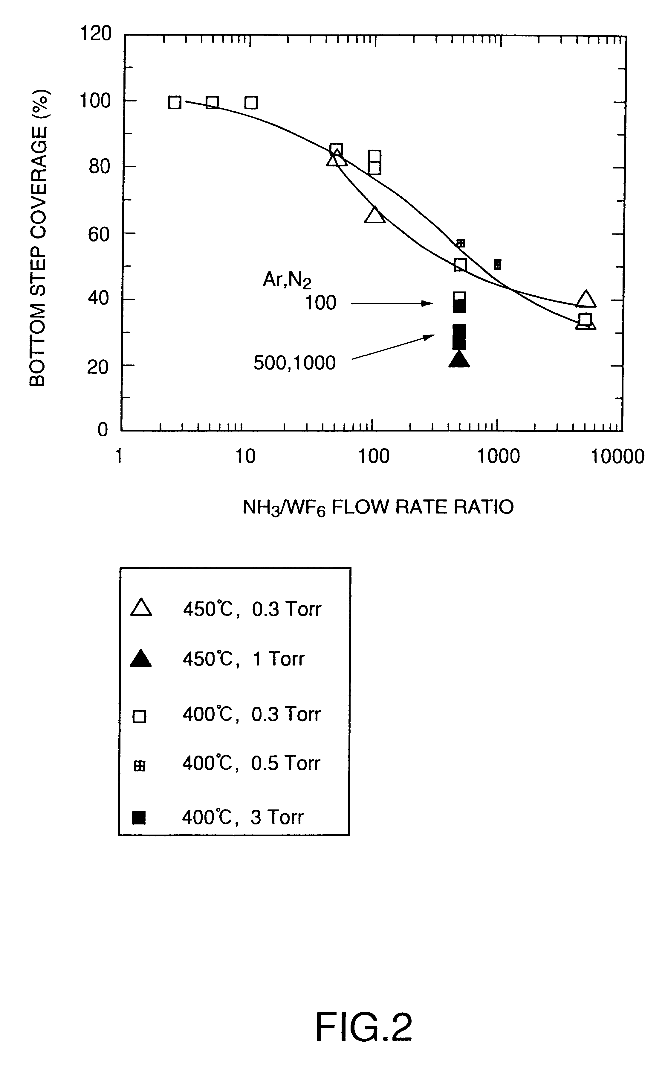
A semiconductor device fabricating method in Example 3 formed a WN.sub.x film and a W film on a poly-Si film by the same process conditions as those in Example 1, except that the susceptor was heated at 456.degree. C. to heat a semiconductor wafer held on the susceptor at 400.degree. C., as shown in Table 1. The semiconductor wafer thus processed was used as Sample 1. Process conditions for Example 3 and measured values of parameters indicating the quality of Sample 1 are tabulated in Table 1. Strength of adhesion of the WN.sub.x film to the poly-Si film was measured by a known measuring method and the condition of Sample 1 after RTA (900.degree. C., 60 s) was examined. Result of examination is shown in Table 1.
example 4
A semiconductor device fabricating method in Example 4 was carried out the same as in Example 3, except that Example 4 continued a film forming process for forming a WN.sub.x film for 20 s. That is, the surface treatment process was carried out to a poly-Si film formed on the semiconductor wafer, a WN.sub.x film was formed on the poly-Si film and a W film was formed on the WN.sub.x film. The semiconductor wafer thus processed was used as Sample 3. Process conditions for Example 4 and the condition of the W / WN.sub.x / poly-Si film after heat treatment are shown in Table 2.
PUM
| Property | Measurement | Unit |
|---|---|---|
| Pressure | aaaaa | aaaaa |
| Pressure | aaaaa | aaaaa |
| Angle | aaaaa | aaaaa |
Abstract
Description
Claims
Application Information