Contact probe

Inactive Publication Date: 2006-07-18
SUMITOMO ELECTRIC IND LTD
View PDF18 Cites 43 Cited by
  • Summary
  • Abstract
  • Description
  • Claims
  • Application Information

AI Technical Summary

Benefits of technology

[0020]A general object of the present invention is to offer a method that secures reliable electrical contact with an electrode hidden underneath an insulating layer, such as a naturally formed oxide layer or resist residues, existing on the surface of a subject surface. Accordingly, a particular object of

Problems solved by technology

Excessive adherence of the shavings 23 diminishes the measurement accuracy, and a good product may be judged as unsatisfactory.
This misjudgment causes an otherwise unnecessary reduction of yield.
The excessive scratches may cause unsatisfactory bonding between the aluminum electrode 22 and a gold wire in the subsequent ultra-sonic bonding process, because the alloying process between the aluminum electrode 22 and the g

Method used


Image

  • Contact probe
  • Contact probe
  • Contact probe

Examples


embodiment 1

(Structure)

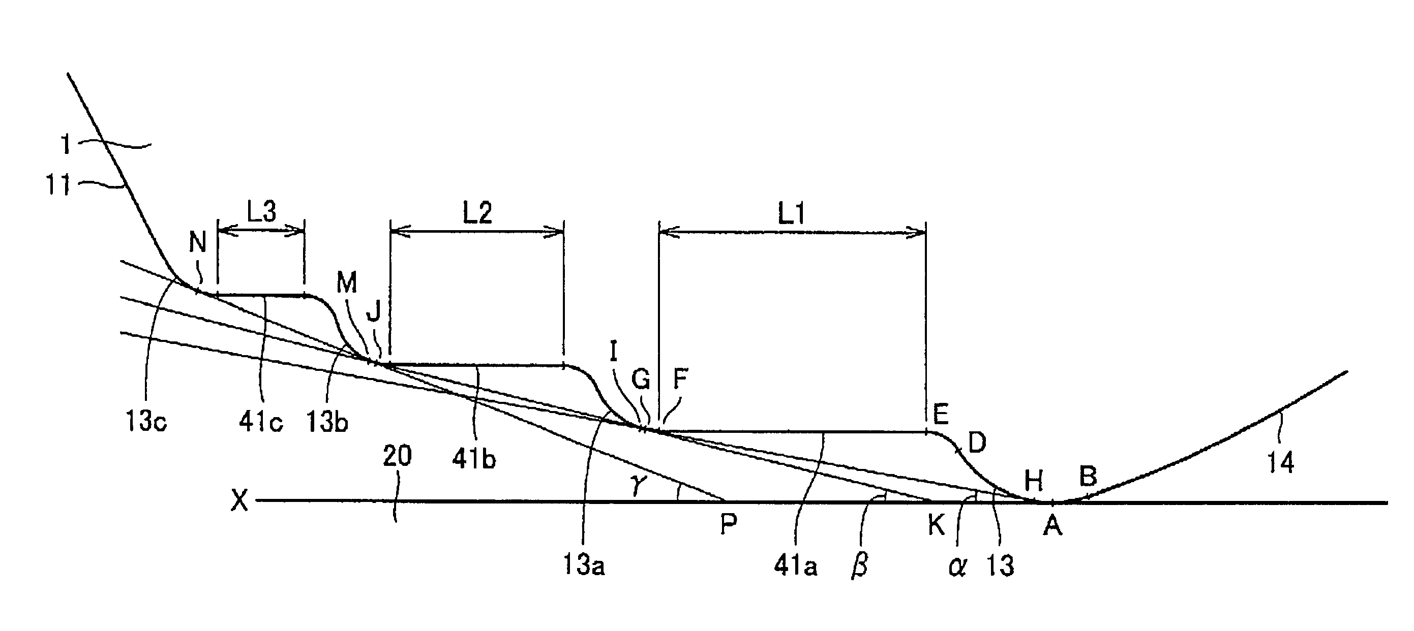
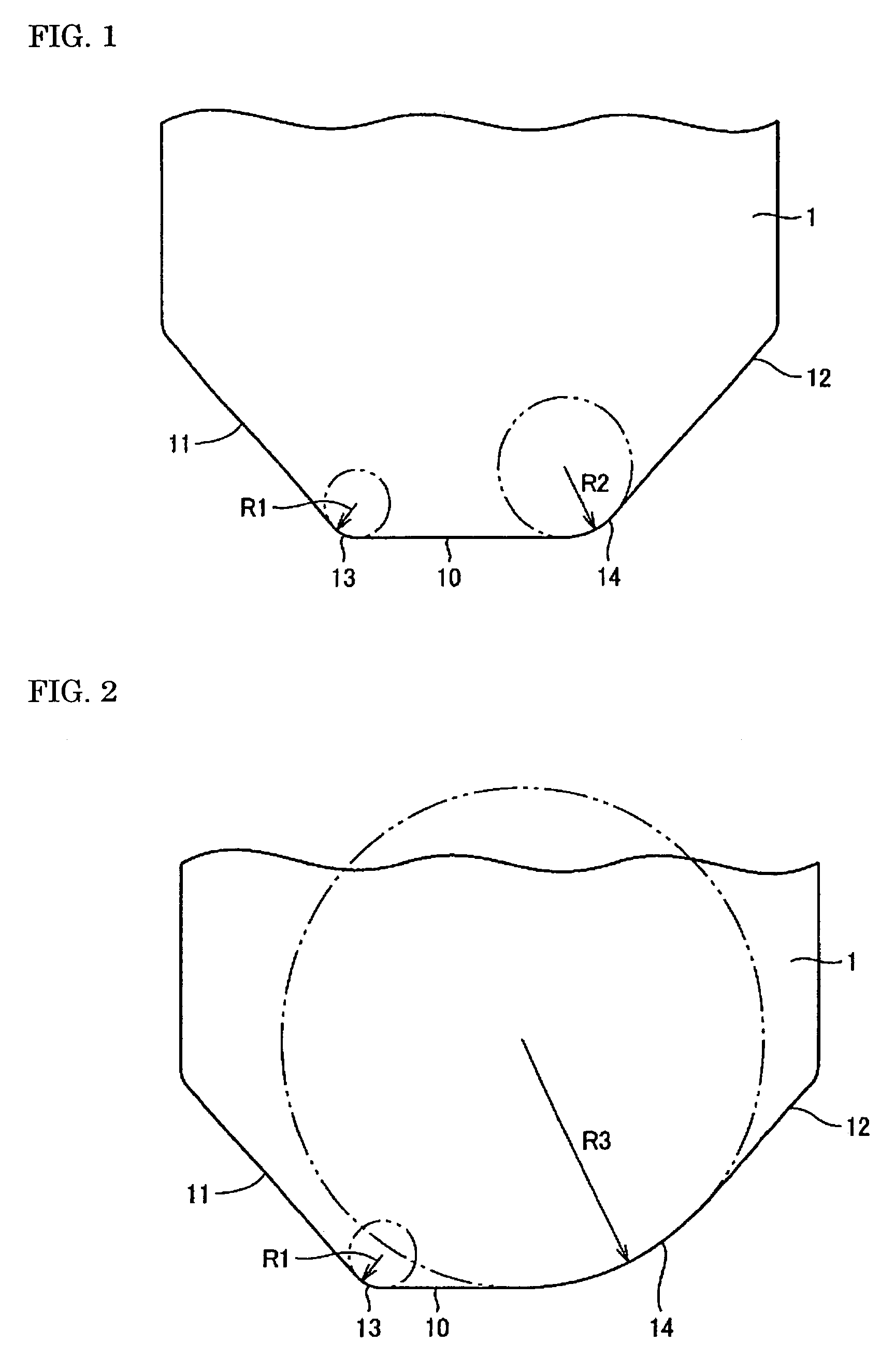
[0094]A contact probe in Embodiment 1 according to the present invention is explained below by referring to FIG. 1. FIG. 1 is an enlarged view of the tip portion 1. In the contact probe, a first oblique face 11 refers to an oblique face that moves in the lead when the tip portion 1 moves for performing the scrubbing by the force pressing the contact probe against the subject surface. As shown in FIG. 1, the first oblique face 11 is located at the left hand side of the contacting flat face 10. The opposite oblique face is referred to as a second oblique face 12. A corner portion 13 through which one end of the contacting flat face 10 is connected to the first oblique face 11 has a radius of curvature different from that of a corner portion 14 through which the other end of the contacting flat face 10 is connected to the second oblique face 12. As can be seen from FIG. 1, the corner portion 14 has the radius of curvature R2 larger than the radius of curvature R1 of the corn...

embodiment 2

(Structure)

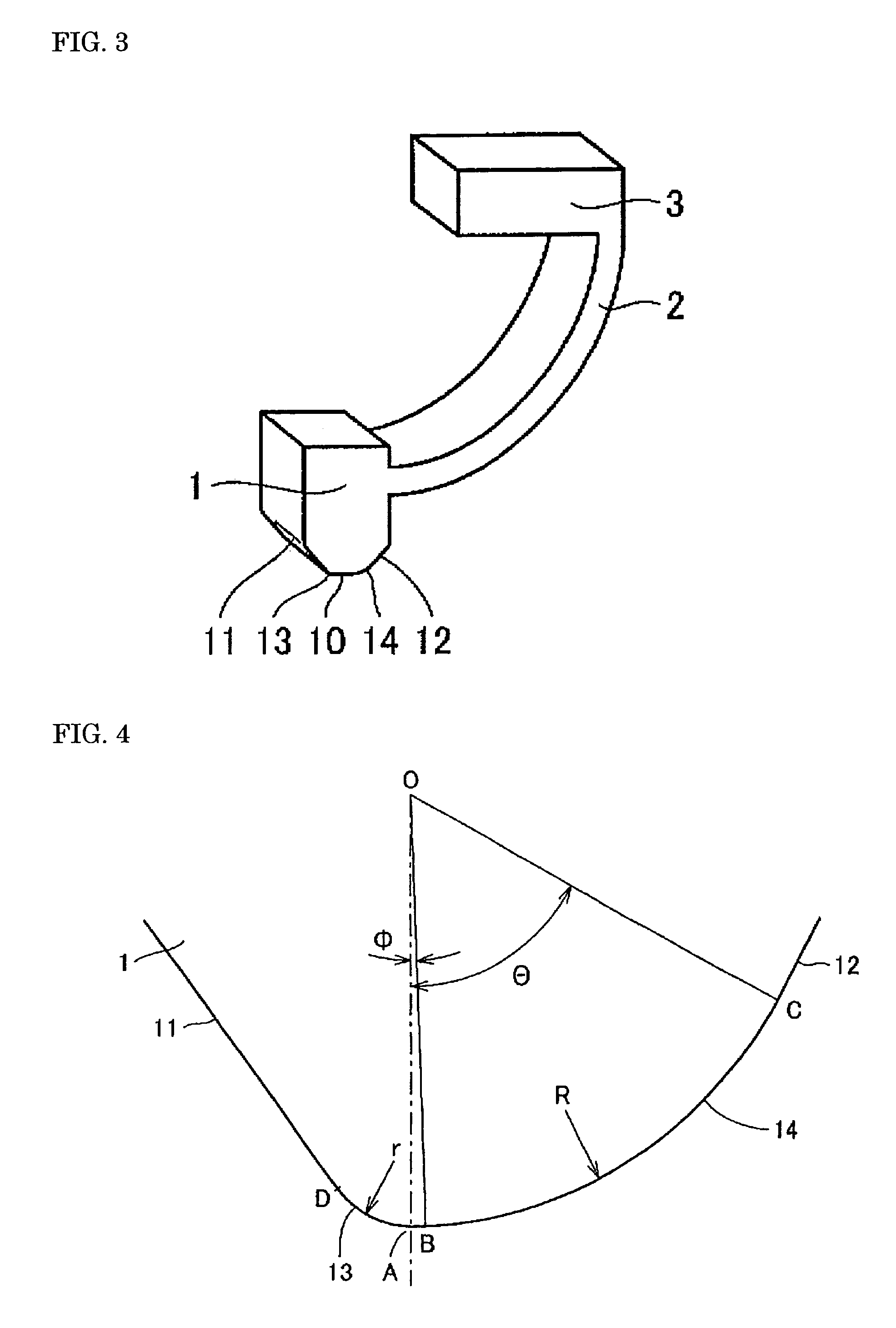
[0099]A contact probe in Embodiment 2 according to the present invention is explained below by referring to FIG. 4. FIG. 4 is an enlarged view of the tip portion 1. During the scrubbing by pressing the contact probe against the subject surface, the tip portion 1 moves to the left in FIG. 4. Hereinafter, the side that moves in the lead in this direction is referred to as “the first side,” and the opposite side (right hand side in FIG. 4) is referred to as “the second side.” Therefore, the second side represents the side that moves in the lead during the scrubbing at the time of the dissociation of the contact probe from the subject surface.

[0100]As shown in FIG. 4, the tip portion 1 of the contact probe has no contacting flat face 10 described in Embodiment 1 (see FIGS. 1 and 2). The tip portion 1 has a corner portion 13 (from point B to point D) as a first corner portion at the first side and a corner portion 14 (from point B to point C) as a second corner portion at the ...

embodiment 3

(Structure)

[0106]A contact probe in Embodiment 3 according to the present invention is explained below by referring to FIG. 5. FIG. 5 is an enlarged view of the tip portion 1. As with the contact probe explained in Embodiment 2, this contact probe has the lowermost point A, a connecting point B, a corner portion 13 as a first corner portion, a corner portion 14 as a second corner portion, a first oblique face 11, a second oblique face 12, and point O as the center of the curvature of the corner portion 14. However, unlike the contact probe in Embodiment 2, the contact probe in Embodiment 3 has a suppressing portion between the corner portion 13 and the first oblique face 11. The suppressing portion is provided to suppress to the subject surface a bulging portion produced from the subject surface by the corner portion 13. The suppressing portion extends from the corner portion 13 toward the first side and includes a suppressing face 41 (from point E to point F) that is opposed to the...


PUM


Abstract

A contact probe comprises a tip portion for making contact with a subject surface, a supporting portion, and a spring portion for connecting the other two members. The tip portion has a corner portion whose radius of curvature is larger than that of the opposite corner portion that moves in the lead during the scrubbing by the pressing force. The insulating layer on the subject surface is sufficiently removed by the scrubbing to secure the electrical contact, and the amount of shavings is minimized during the dissociation of the contact probe. Formation of scratches on the subject surface is reduced. Another contact probe for a ball-shaped electrode has a tip portion with a recess, which has a protrusion and bottom. The protrusion breaks the insulating layer on the electrode to secure the electrical contact. The bottom makes contact with the electrode to prevent the protrusion from excessively biting the electrode.

Description

RELATED APPLICATION[0001]This application is a 371 of PCT / JP 02 / 10563 filed on Oct. 10, 2002 under No. PCT / JP02 / 10563.TECHNICAL FIELD[0002]The present invention relates to a contact probe for electrically inspecting semiconductor substrates, liquid-crystal displaying devices, and other devices.BACKGROUND ART[0003]Inspection of the electric circuits formed for semiconductor substrates, liquid-crystal displaying devices, and other devices is usually conducted by using an inspecting apparatus provided with a multitude of contact probes. The surface of a circuit to be measured (hereinafter referred to as a subject surface) is usually covered by an insulating layer, such as a naturally formed oxide layer or resist residues. To carry out the inspection, it is necessary to break the insulating layer to secure reliable electrical contact with the electrode of the circuit underneath the insulating layer. Two methods have been employed to break the insulating layer. One is to scrub along the ...

Claims


Application Information

Patent Timeline
IPC IPC(8): G01R31/02G01R31/26G01R1/067
CPCG01R1/06738G01R1/067
Inventor HAGA, TSUYOSHISHIMADA, SHIGEKIKIMURA, ATSUSHI
Owner SUMITOMO ELECTRIC IND LTD
Why Eureka
Try Eureka