Enhanced deposition of noble metals

Active Publication Date: 2007-02-15
ASM INTERNATIONAL
View PDF98 Cites 83 Cited by
  • Summary
  • Abstract
  • Description
  • Claims
  • Application Information

AI Technical Summary

Benefits of technology

[0011] Thin films of noble metals can be deposited by vapor deposition processes, such as atomic layer deposition (ALD) type processes. In some embodiments, in each ALD cycle the substrate is alternately contacted with a noble metal precursor and a second reactant, such that a thin noble metal film is formed on the

Problems solved by technology

In particular on metal oxides and metal nitrides, the incubation time can be long.
The long incubation time uses up expensive noble metal precursor and increases processing time.
This can be a particular problem in the deposition of noble metal films in an ALD batch system, where 50-100 wafers are processed at the same time.
Unfortunately the PEALD process

Method used


Image

  • Enhanced deposition of noble metals
  • Enhanced deposition of noble metals
  • Enhanced deposition of noble metals

Examples


Example

EXAMPLE 1

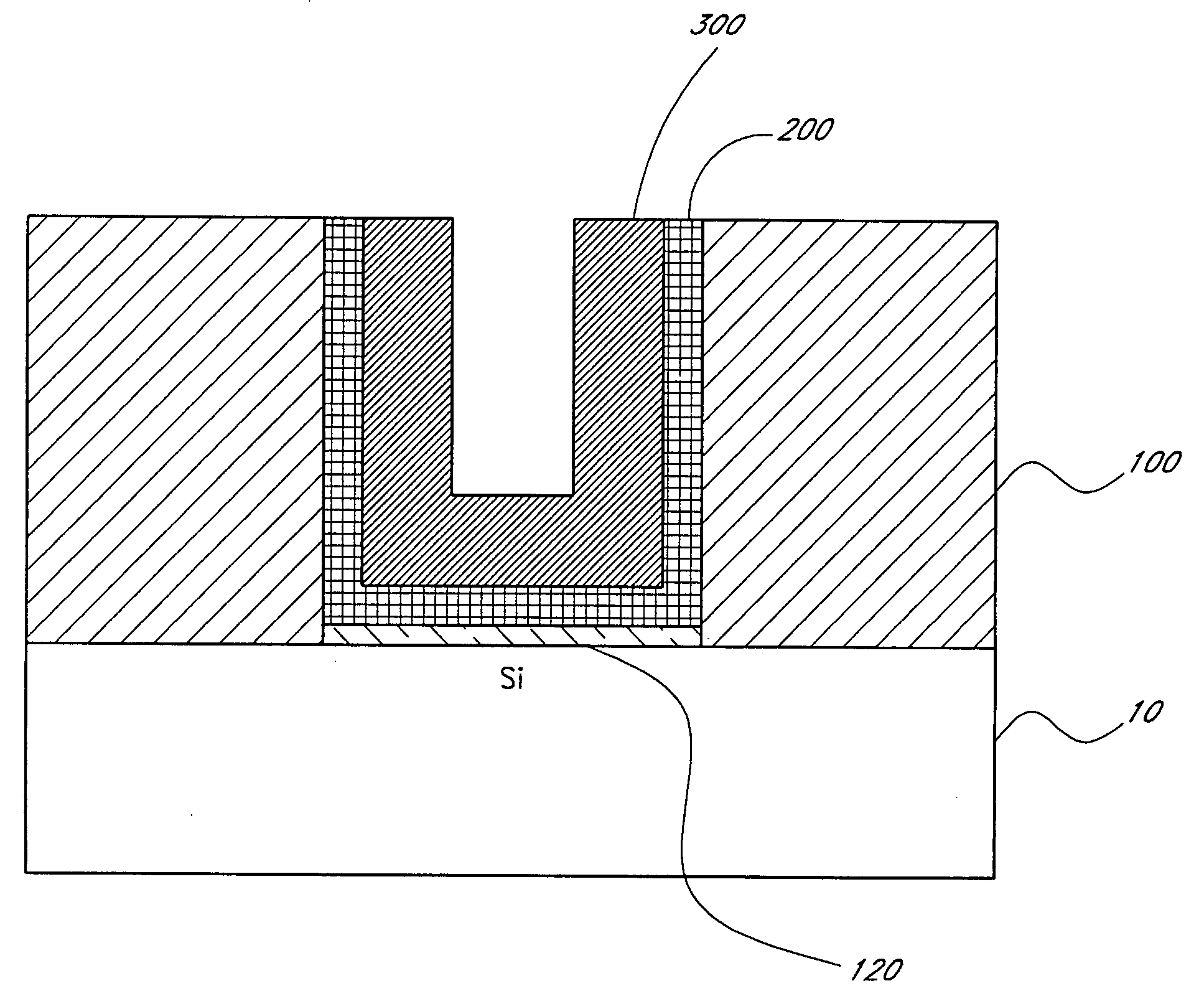
[0105] Ruthenium thin films were deposited on 300 mm wafers from alternating pulses of bis(ethylcyclopentadienyl)ruthenium (Ru(EtCp)2) and oxygen (O2) at a temperature of about 370° C. No halide treatment was employed.

[0106] The pulse length of the evaporated ruthenium precursor was about 0.7 seconds and was followed by a purge with an inert gas that lasted from about 2 seconds. The pulse length of the oxygen-containing reactant was about 2 seconds and the purge thereafter was about 2 seconds.

[0107] Ruthenium was found to grow using this process on TaN, Al2O3, Ta and HfO2 surfaces. The typical growth rate is about from 0.5 to 0.9 Å / cycle on these surfaces, not counting incubation time. The incubation time for Ru growth was found to be about 50-100 cycles on TaN, 50-100 cycles on Al2O3, about 50 cycles on Ta and virtually zero on HfO2.

[0108] However, even 450 cycles of the same Ru process did not produce a measurable and conductive film on a thermal silicon oxide surface...

Example

EXAMPLE 2

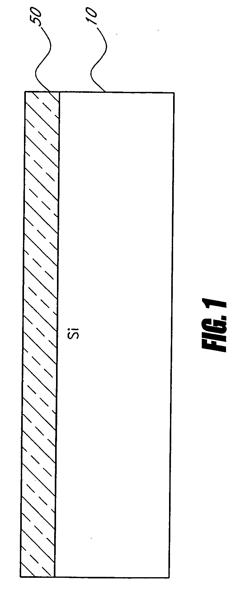
[0110] Ruthenium thin films were deposited from alternating pulses of bis(ethylcyclopentadienyl)ruthenium (Ru(EtCp)2) and oxygen (O2) on a pure SiO2 surface and on a SiO2 surface modified with HfCl4. The reactions were carried out at 260° C. to 360° C. On the pure SiO2 surface, some color began to be seen at 360° C. The low intensity of the color and the fact that the whole SiO2 surface was not covered with the color indicated that only some weak reaction of the ruthenium precursor and the SiO2 surface was occurring at this temperature.

[0111] At the lower temperature (260° C.) the SiO2 surface remained completely white, indicating that no ruthenium growth was taking place. These results are consistent with those of Example 1 and indicate that Ru(EtCp)2 is not reactive with a pure silicon surface at temperatures below about 360° C.

[0112] These results confirm that Ru(EtCp)2 is highly unreactive towards a pure SiO2 surface and explain the long incubation time that has been...

Example

EXAMPLE 3

[0114] Bis(ethylcyclopentadienyl)ruthenium (Ru(EtCp)2) was used to deposit ruthenium by ALD on pure, untreated Al2O3 and on Al2O3 that had been treated with HfCl4 or AlCl3.

[0115] The ALD reactions were carried out at both 260° C. and 360° C. At the higher temperature, only some non-uniform brownish color was observed on the untreated surface. At the lower temperature, the untreated Al2O3 surface remained unchanged by the deposition process.

[0116] On both the HfCl4 and AlCl3 treated surfaces, a uniform brown film was obtained at both temperatures. At the lower temperature the film was smoother than at the higher temperature.

[0117] Although the foregoing invention has been described in terms of certain preferred embodiments, other embodiments will be apparent to those of ordinary skill in the art. Moreover, although illustrated in connection with particular process flows and structures, the skilled artisan will appreciate variations of such schemes for which the methods d...


PUM

PropertyMeasurementUnit
Temperatureaaaaaaaaaa

Abstract

The invention relates generally to processes for enhancing the deposition of noble metal thin films on a substrate by atomic layer deposition. Treatment with gaseous halides or metalorganic compounds reduces the incubation time for deposition of noble metals on particular surfaces. The methods may be utilized to facilitate selective deposition. For example, selective deposition of noble metals on high-k materials relative to insulators can be enhanced by pretreatment with halide reactants. In addition, halide treatment can be used to avoid deposition on the quartz walls of the reaction chamber.

Description

REFERENCE TO RELATED APPLICATIONS [0001] The present application claims priority to U.S. Provisional Application No. 60 / 662,145, filed Mar. 15, 2005 and is related to U.S. Provisional Application No. 60 / 662,144, filed Mar. 15, 2005, each of which is incorporated herein by reference.BACKGROUND OF THE INVENTION [0002] 1. Field of the Invention [0003] Noble metal thin films can be deposited by vapor deposition processes, such as atomic layer deposition. Such films find use, for example, in integrated circuits and magnetic recording media. [0004] 2. Description of the Related Art [0005] Thin films of ruthenium and other noble metals can be used in a wide variety of applications including integrated circuits and magnetic recording media. For example, noble metals such as ruthenium and metal alloys comprising noble metals, such as RuTa, may be used as an electrode material in transistors, particularly those where silicon oxide is replaced by high-k dielectrics. Noble metals can also be us...

Claims


Application Information

Patent Timeline
IPC IPC(8): C23C16/00
CPCC23C16/0218C23C16/18C23C16/08H01L21/28562C23C16/45525
Inventor HAUKKA, SUVI P.TUOMINEN, MARKO J.RAHTU, ANTTI
Owner ASM INTERNATIONAL
Why Eureka
Try Eureka