Method for depositing microcrystalline silicon and monitor device of plasma enhanced deposition

Active Publication Date: 2011-06-09
IND TECH RES INST
View PDF14 Cites 3 Cited by
  • Summary
  • Abstract
  • Description
  • Claims
  • Application Information

AI Technical Summary

Benefits of technology

The invention provides a method for depositing a microcrystalline silicon film, comprising performance of an open loop and a close loop plasma enhanced deposition process without and with modulating process parameters, respectively. A film is deposited by the open loop plasma enhanced deposition process till a film crystallinity is stable and then b

Problems solved by technology

However, the deposition rate of the microcrystalline silicon is low (about 2 Å/sec), thus becoming a bottleneck during application.
Such low deposition rate is more problematic for large area depositing processes because crystallinity uniformity is concerned.
Therefore, the low throughput of depositing microcrystalline silicon resulting in

Method used


Image

  • Method for depositing microcrystalline silicon and monitor device of plasma enhanced deposition
  • Method for depositing microcrystalline silicon and monitor device of plasma enhanced deposition
  • Method for depositing microcrystalline silicon and monitor device of plasma enhanced deposition

Examples


Example

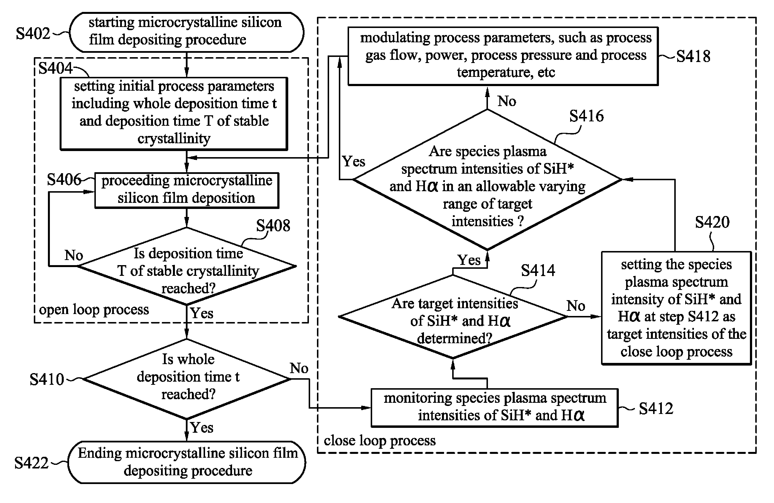
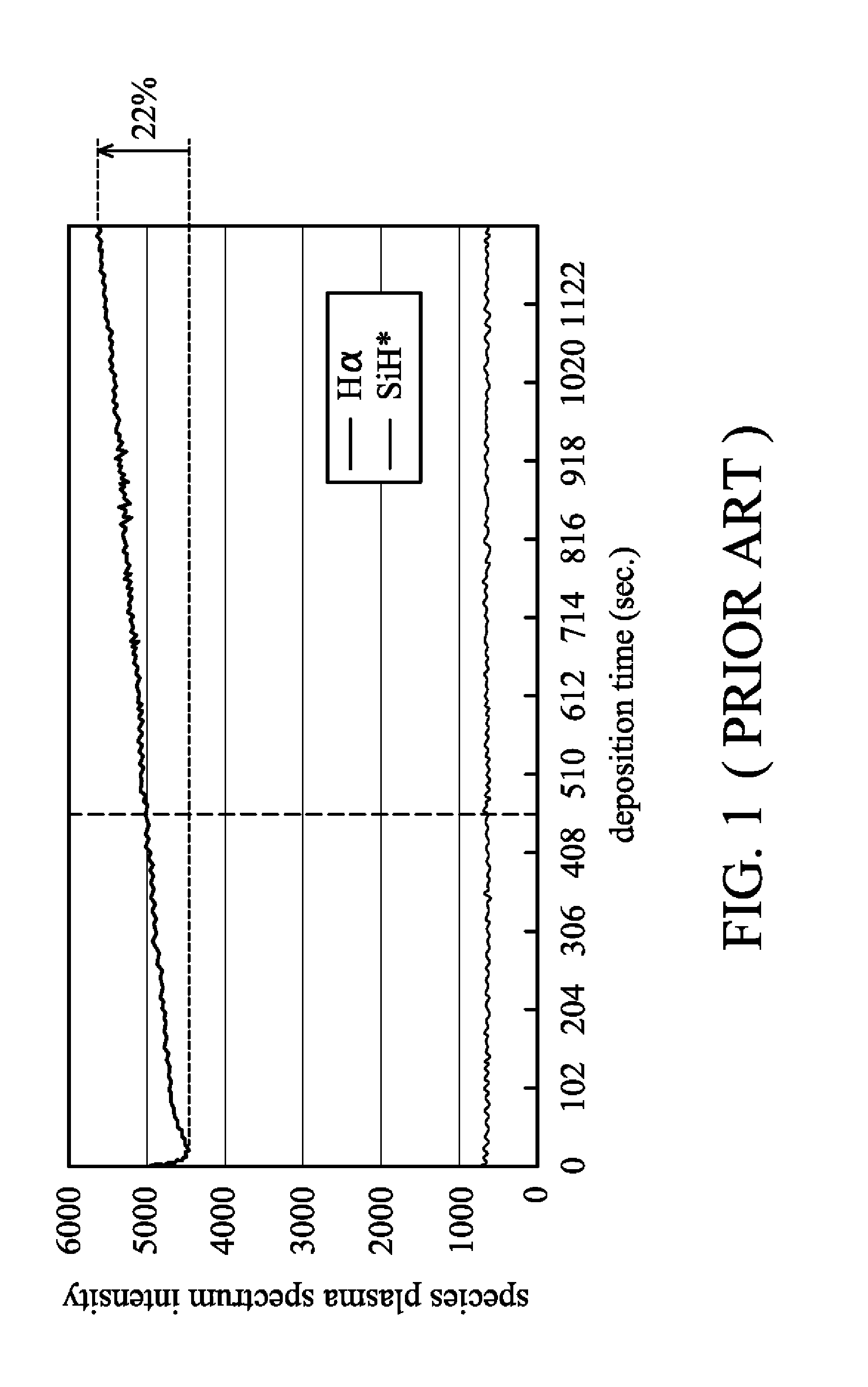
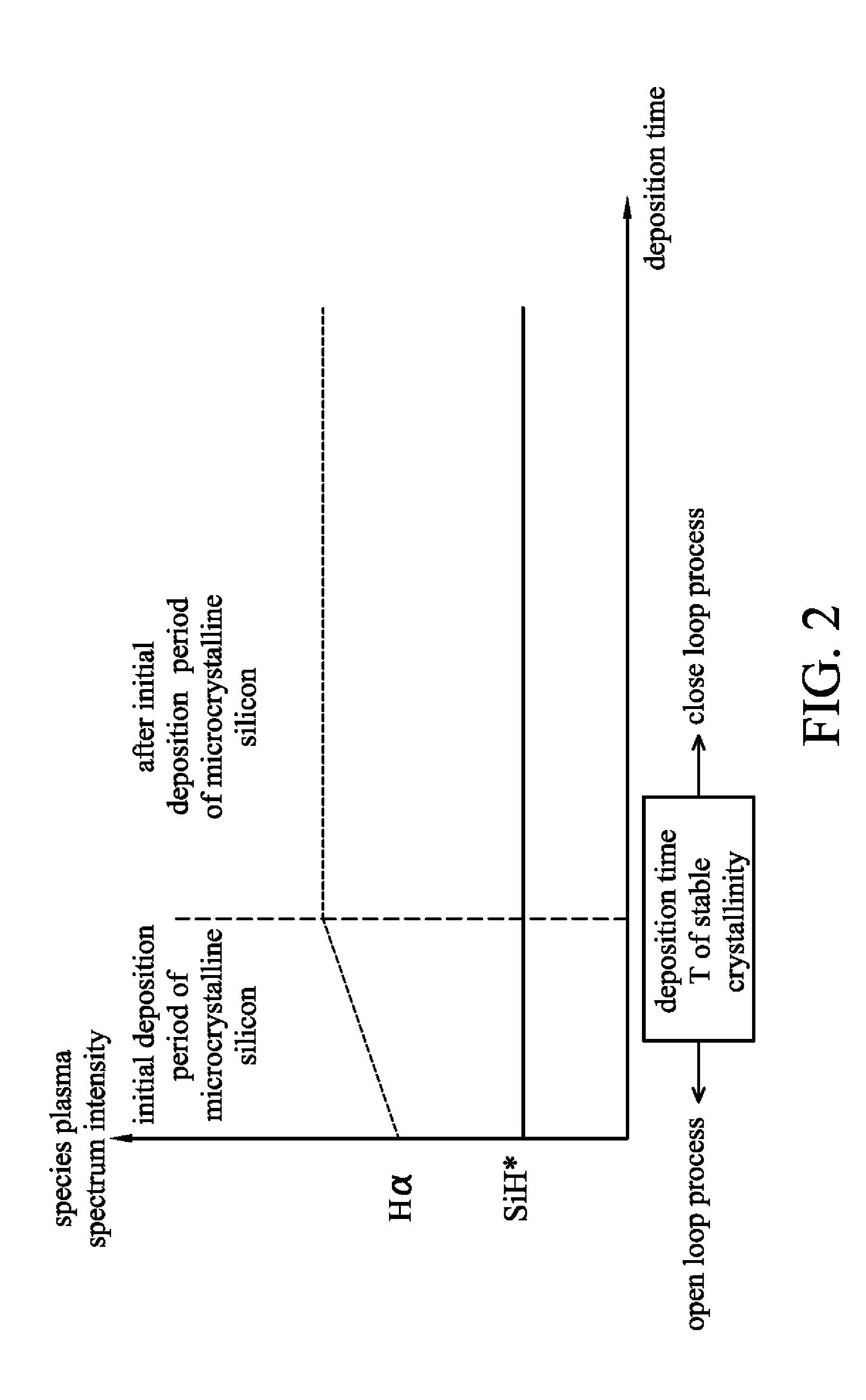
First, the growth mechanism of microcrystalline silicon is illustrated from a thin film engineering aspect. Growth mechanism of a microcrystalline silicon film comprises several stages as follows: species SiHx absorbing onto a substrate, diffusing to cluster for nucleation, nuclear growth, forming continuous film and growth of film. The species H provides hydrogen etching effect on the film to get the required crystallinity. During an open loop process of depositing microcrystalline silicon in PECVD, a process gas is dissociated in the plasma field to form species SiHx and H, wherein SiHx is a source of thin film growth and H has function of hydrogen etching to achieve the required crystallinity. However, if the amount of species H increased up exceedingly, SiHx would be diluted and growth rate of microcrystalline silicon thin film is reduced. FIG. 1 shows plasma spectrum intensity as a function of depositing time of SiH* (i.e. species SiHx concentration) and Hα (i.e. species H conc...


PUM


Abstract

A method for depositing a microcrystalline silicon film is disclosed, including performing an open loop and close loop plasma enhanced deposition process without and with modulating process parameters, respectively. A film is deposited by the open loop plasma enhanced deposition process till a required film crystallinity and then performing a closed loop plasma enhanced deposition process which monitors species plasma spectrum intensities SiH* and Hα and modulates process parameters of the plasma enhanced deposition process resulting in the species concentration stabilization which controls the intensities variation of SiH* and Hα within an allowed range of a target value for improving film depositing rate.

Description

CROSS REFERENCEThis Application claims priority of Taiwan Patent Application No. 098141847, filed on Dec. 8, 2009, the entirety of which is incorporated by reference hereinBACKGROUND OF THE INVENTION1. Field of the InventionThis invention generally relates to a thin film depositing technology and more particularly relates to a method for depositing microcrystalline silicon.2. Description of the Related ArtA tandem silicon thin film solar cell generally uses microcrystalline silicon which has an advantage to increase photoelectric conversion efficiency of solar cells. The microcrystalline silicon is generally fabricated by plasma enhanced chemical vapor deposition (PECVD). However, the deposition rate of the microcrystalline silicon is low (about 2 Å / sec), thus becoming a bottleneck during application. Specifically, a thin film solar cell generally requires a microcrystalline silicon having thickness of about 1-2 μm, such that the depositing time often exceeds one hour. Such low depo...

Claims


Application Information

Patent Timeline
IPC IPC(8): H01L21/66B05C11/00
CPCH01J37/32935H01L21/0262H01L21/02532H01J37/32972
Inventor DU, CHEN-CHUNGLEE, SHENG-LANGLIANG, MUH-WANGHUANG, JEN-RONGCHANG, CHIA-HAO
Owner IND TECH RES INST
Why Eureka
Try Eureka