Methods of filling gaps and methods of depositing materials using high density plasma chemical vapor deposition

Inactive Publication Date: 2005-03-24
MICRON TECH INC
View PDF14 Cites 3 Cited by
  • Summary
  • Abstract
  • Description
  • Claims
  • Application Information

AI Technical Summary

Benefits of technology

[0007] In one aspect, the invention encompasses a method of providing an improved deposition rate uniformity. A material is deposited over a surface in the presence of at least one gas selected from the group consisting of D2, HD, DT; T2 and TH. An overall deposition rate during the depositing is defined by a ratio of deposition of the material relative to a simultaneous rate of etch of the material. The overall deposition rate has a degree of variance across the surface which is measurably improved relative to a corresponding degree of variance that occurs during deposition utilizing H2 under otherwise substantially identical conditions.

Problems solved by technology

As feature size of devices decreases, widths of gaps to be filled also decreases and aspect ratio of such gaps can become very high.
Accordingly, minimization of void area within gap-fill becomes more difficult but increasingly important for effective isolation.
The variance in deposition rate across a surface can make optimizing deposition conditions and parameters for void exclusion difficult if not impossible.

Method used


Image

  • Methods of filling gaps and methods of depositing materials using high density plasma chemical vapor deposition
  • Methods of filling gaps and methods of depositing materials using high density plasma chemical vapor deposition
  • Methods of filling gaps and methods of depositing materials using high density plasma chemical vapor deposition

Examples


Embodiment Construction

[0018] This disclosure of the invention is submitted in furtherance of the constitutional purposes of the U.S. Patent Laws “to promote the progress of science and useful arts” (Article 1, Section 8).

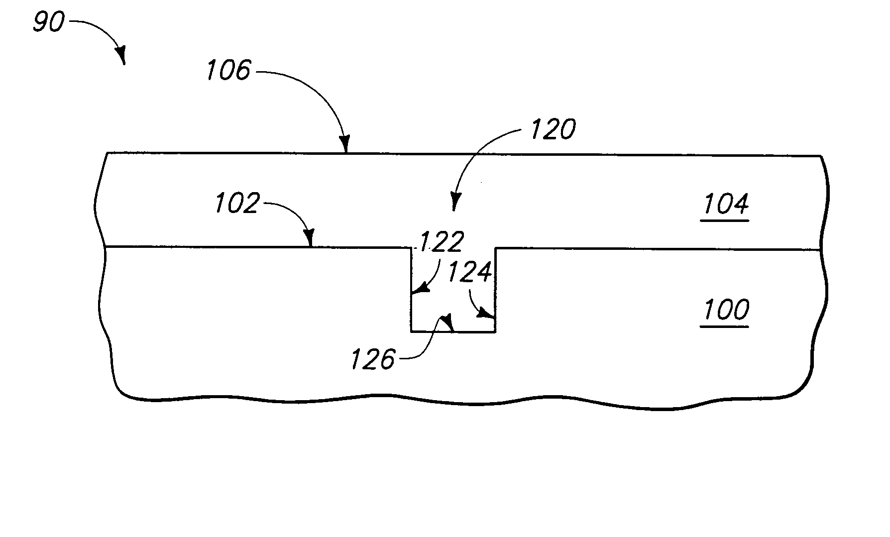
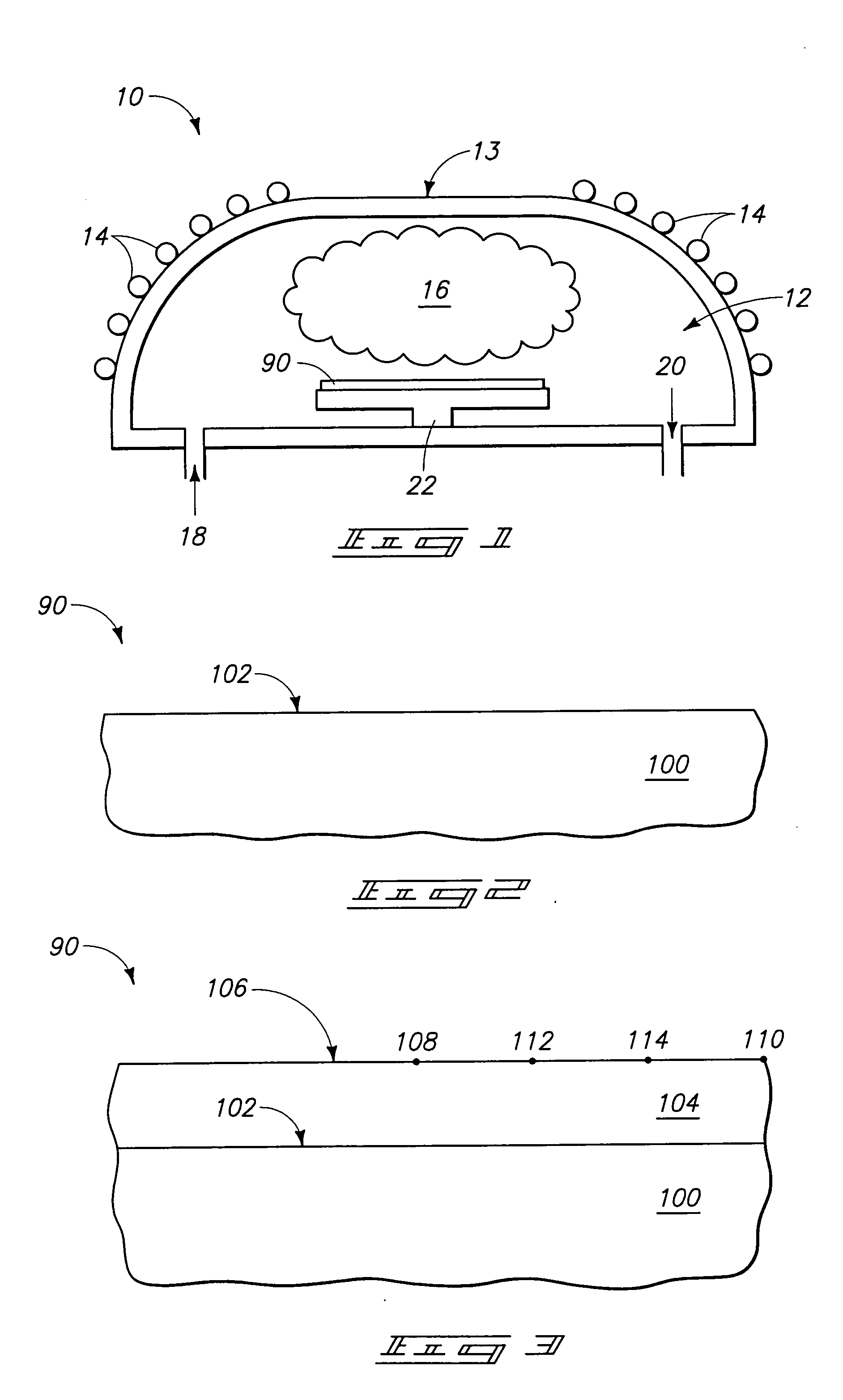
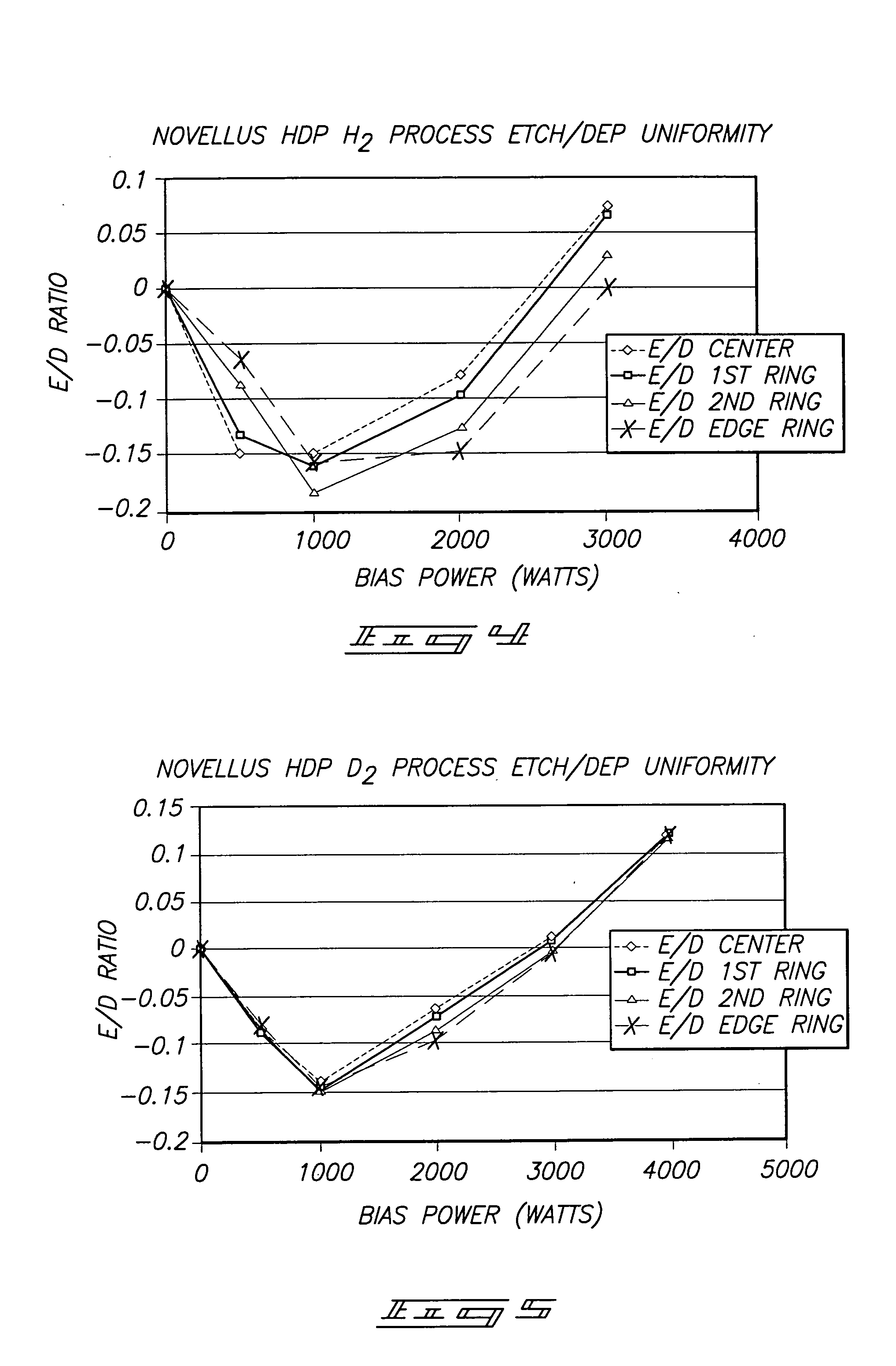
[0019] The invention encompasses an improved method of depositing layers over a substrate. The layers can be deposited by chemical vapor deposition utilizing one or more heavy-hydrogen compounds. For purposes of the present description, the term heavy-hydrogen can refer to deuterium (D) or tritium (T), and the term heavy-hydrogen compound can refer to a compound having one, some or all hydrogen atoms replaced with D and / or T above the level of natural abundance for the corresponding heavy isotope. More specifically, silicon-comprising layers can be formed by high density plasma chemical vapor deposition (HDP-CVD) in the presence of a heavy-hydrogen sputtering gas, a heavy-hydrogen comprising precursor compound, or both a heavy-hydrogen precursor and a heavy-hydrogen sputtering gas.

[002...


PUM

PropertyMeasurementUnit
Fractionaaaaaaaaaa
Poweraaaaaaaaaa
Diameteraaaaaaaaaa

Abstract

The invention includes a method of filling gaps in a semiconductor substrate. A substrate and a gas mixture containing at least one heavy-hydrogen compound are provided within a reaction chamber. The gas mixture is reacted to form a layer of material over the substrate by simultaneous deposition and etch of the layer. The layer of material fills the gap such that the material within the gap is essentially void-free. The invention includes a method of providing improved deposition rate uniformity. A material is deposited over a surface in the presence of at least one gas selected from the group consisting of D2, HD, DT, T2 and TH. The net deposition rate during the deposition has a degree of variance across the surface which is measurably improved relative to a corresponding degree of variance that occurs during deposition utilizing H2 under otherwise substantially identical conditions.

Description

TECHNICAL FIELD [0001] The invention pertains to methods of forming a layer over a substrate, and in particular embodiments pertains to methods of filling a gap. BACKGROUND OF THE INVENTION [0002] Insulative materials and layers of insulative materials are used extensively in various semiconductor applications to insulate or electrically isolate structural features and circuit elements. The insulative properties of such materials and layers can often be affected by the ability to minimize or exclude void areas formed during the deposition of the insulative material. Uniformity of deposition rates across a deposited layer during deposition can influence film quality and ability to effectively minimize void inclusion. As feature size of devices decreases, widths of gaps to be filled also decreases and aspect ratio of such gaps can become very high. Accordingly, minimization of void area within gap-fill becomes more difficult but increasingly important for effective isolation. The vari...

Claims


Application Information

Patent Timeline
IPC IPC(8): C23C16/04C23C16/40H01L21/316H01L21/762H01L21/768
CPCC23C16/045C23C16/401H01L21/02126H01L21/02164H01L21/76837H01L21/02274H01L21/31612H01L21/31625H01L21/76224H01L21/02211H01L21/02129
Inventor RUEGER, NEAL R.BUDGE, WILLIAMLI, WEIMINSANDHU, GURTEJ S.
Owner MICRON TECH INC
Why Eureka
Try Eureka