Structure for microelectronic packaging with bond elements to encapsulation surface

a technology of encapsulation surface and structure, applied in the direction of printed circuit non-printed electric components association, sustainable manufacturing/processing, final product manufacturing, etc., can solve the problem of appreciable vertical gap between

Active Publication Date: 2014-11-04
INVENSAS CORP
View PDF470 Cites 111 Cited by
  • Summary
  • Abstract
  • Description
  • Claims
  • Application Information

AI Technical Summary

Problems solved by technology

In addition, because the substrate of the higher package in the stack sits above the dielectric overmold in the next lower package, there is an appreciable gap in the vertical direction between the terminals of the higher package and the stacking contacts of the lower package.

Method used


Image

  • Structure for microelectronic packaging with bond elements to encapsulation surface
  • Structure for microelectronic packaging with bond elements to encapsulation surface
  • Structure for microelectronic packaging with bond elements to encapsulation surface

Examples


Embodiment Construction

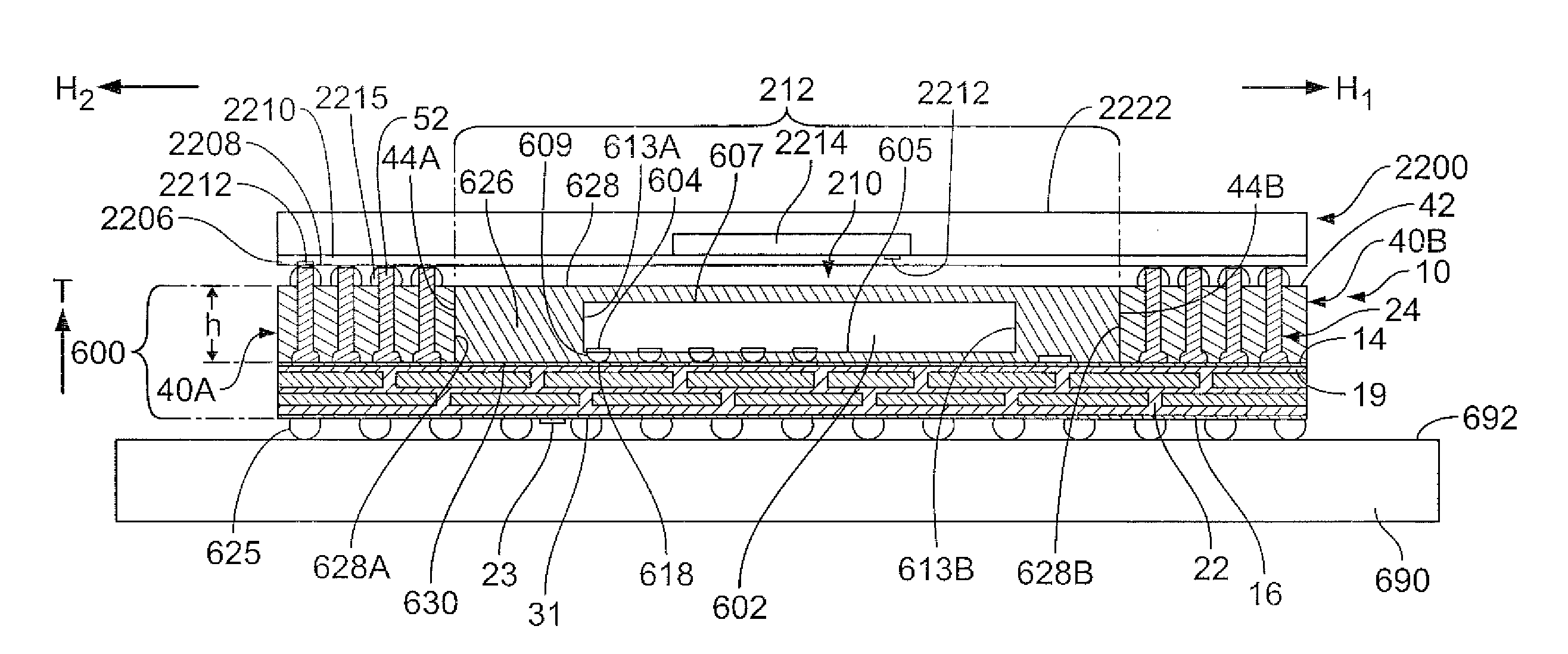
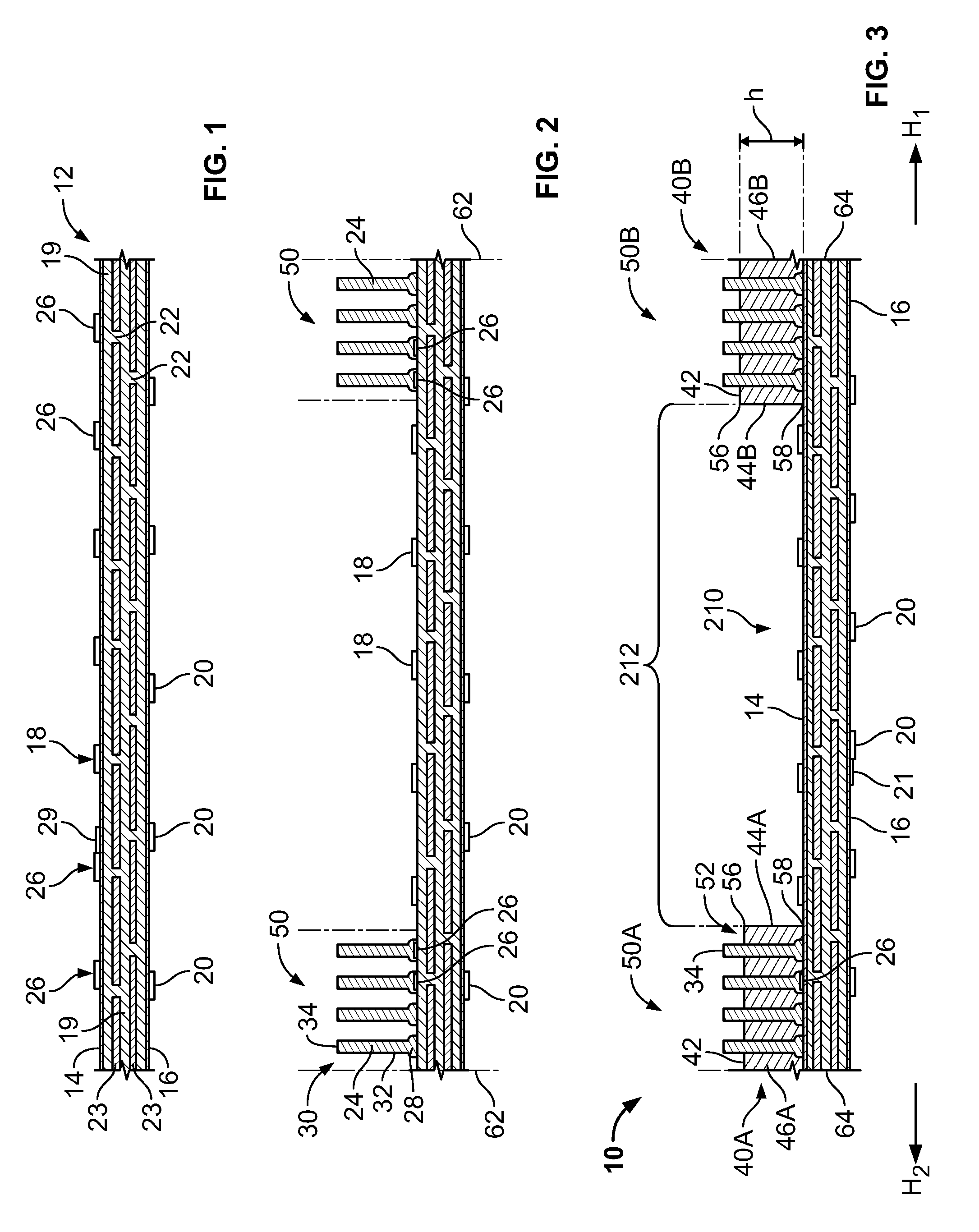
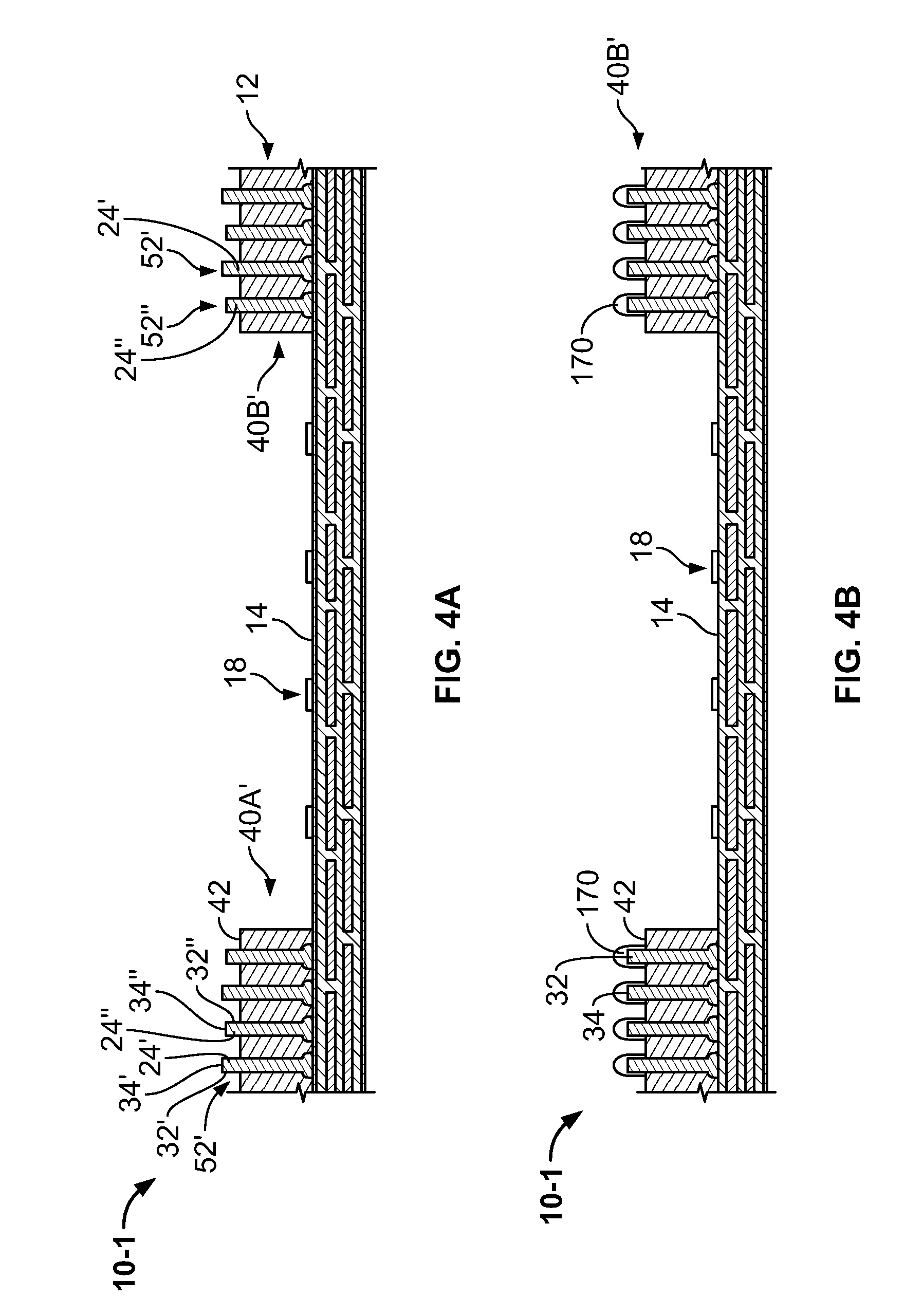
[0041]A structure 10 (see FIG. 3) according to one embodiment of the disclosure may include a substrate 12 (see FIG. 1) having a first surface 14 and a second surface 16. The substrate 12 typically is in the form of a dielectric element, which is substantially flat. The dielectric element may be sheet-like and thin. In particular embodiments, the dielectric element may include one or more layers 23 of organic dielectric material or composite dielectric materials, such as, without limitation: polyimide, polytetrafluoroethylene (“PTFE”), epoxy, epoxy-glass, FR-4, BT resin, thermoplastic, or thermoset plastic materials. The first surface 14 and second surface 16 are preferably substantially parallel to each other and are spaced apart at a distance perpendicular to the surfaces 14 and 16 defining the thickness of the substrate 12. The thickness of substrate 12 is preferably within a range of generally acceptable thicknesses for the present application. In an embodiment, the distance bet...


PUM


Abstract

A structure may include bond elements having bases joined to conductive elements at a first portion of a first surface and end surfaces remote from the substrate. A dielectric encapsulation element may overlie and extend from the first portion and fill spaces between the bond elements to separate the bond elements from one another. The encapsulation element has a third surface facing away from the first surface. Unencapsulated portions of the bond elements are defined by at least portions of the end surfaces uncovered by the encapsulation element at the third surface. The encapsulation element at least partially defines a second portion of the first surface that is other than the first portion and has an area sized to accommodate an entire area of a microelectronic element. Some conductive elements are at the second portion and configured for connection with such microelectronic element.

Description

FIELD OF THE INVENTION[0001]The present invention relates to structures for microelectronic packaging.BACKGROUND OF THE INVENTION[0002]Microelectronic elements such as semiconductor chips commonly are provided with elements which protect the microelectronic element and facilitate its connection to other elements of a larger circuit. For example, a semiconductor chip typically is provided as a small, flat element having oppositely facing front and rear surfaces and contacts at the front surface. The contacts are electrically connected to the numerous electronic circuit elements formed integrally within the chip. Such a chip most commonly is provided in a package having a miniature circuit panel referred to as a substrate. The chip is typically mounted to the substrate with the front or rear surface overlying a surface of the substrate, and the substrate typically has terminals at a surface of the substrate. The terminals are electrically connected to the contacts of the chip. The pac...

Claims


Application Information

Patent Timeline
Patent Type & Authority Patents(United States)
IPC IPC(8): H01L21/00H05K1/18H01L23/02H01L23/00H01L23/528
CPCH01L2225/1023H05K2201/10515H05K1/141H01L24/11H05K2201/042H05K2201/10318H05K1/181H01L25/03H01L2224/17051H05K2201/10977H05K2203/049H01L2224/1403H01L25/105H01L2225/1058H01L23/528H01L2224/14051H01L2225/06517H01L2225/06513H01L2224/1191H01L24/03H01L2224/1703H05K2201/10962H05K2201/09609H01L23/3157H05K2201/10287H01L23/49811H01L2224/11334H01L25/0657H05K1/185H05K2201/10242H01L2224/13076H01L2224/48227H01L2924/15311H01L24/14H01L2224/48091H01L2924/19107H01L23/3135H01L2224/13082H01L24/13H01L2224/16145H01L2224/14135H01L2924/15321H01L2224/16225H01L23/3128H01L2224/131H01L2224/13017H01L2224/16105H01L2224/13022H01L24/17H01L2924/15322H01L24/16H01L2224/32225H01L21/56H01L2224/73265H01L21/561H01L2224/16227H01L2224/10126H01L24/45H01L24/48H01L24/73H01L2224/13101H01L2224/45012H01L2224/45014H01L2224/45015H01L2224/45101H01L2224/45124H01L2224/45144H01L2224/45147H01L2224/45155H01L2224/45624H01L2224/45655H01L2224/73204H01L2924/12042H01L2224/1134H01L2225/1041H01L2924/181H01L2924/00014Y02P70/50H01L2924/00012H01L2924/014H01L2924/00H01L2924/206H05K1/11H05K1/0298
Inventor HABA, BELGACEMMOHAMMED, ILYASCASKEY, TERRENCECHAU, ELLIS
Owner INVENSAS CORP
Why Eureka
Try Eureka