
Method and apparatus for manufacturing a semiconductor device

a semiconductor device and manufacturing method technology, applied in the direction of grinding drives, manufacturing tools, grinding machine components, etc., can solve the problems of reducing mechanical strength, reducing the efficiency of manufacturing, affecting the quality of manufacturing, so as to prevent the wafer from chipping and cracking. , the effect of safe and sure picking up

Active Publication Date: 2014-11-18
FUJI ELECTRIC CO LTD
View PDF24 Cites 2 Cited by
  • Summary
  • Abstract
  • Description
  • Claims
  • Application Information

AI Technical Summary

Benefits of technology

[0038]In some embodiments, a wafer can be safely and surely picked up and transported smoothly to the predetermined destination preventing the wafer from chipping and cracking.

Problems solved by technology

The reduction in wafer thickness, however, in certain circumstances, may cause a break at the peripheral edge of the wafer resulting in chipping of the wafer.
Because thin wafers can show lowered mechanical strength, a problem can also arise that the wafer is liable to generate cracks, breakage, and deflection.
These problems are noticeable in wafers with a large diameter, in particular.
Thin and large diameter wafers showing large deflection have difficulties in transporting the wafer between manufacturing steps and in positioning the wafer on manufacturing devices.
Hence, the above-mentioned problems can cause difficulty in carrying out these steps on the back surface of the wafer.
This means, however, leaves the problem to reduce the time required for picking up the wafer unsolved and lowers the efficiency of the transport operation.
Thus, the problem to pick up the wafer with no damage is left unsolved.
Stress concentration is liable to be developed especially at places damaged by the grindstone in the grinding step and places with varied curvature.

Method used


Image

  • Method and apparatus for manufacturing a semiconductor device
  • Method and apparatus for manufacturing a semiconductor device
  • Method and apparatus for manufacturing a semiconductor device

Examples


first embodiment

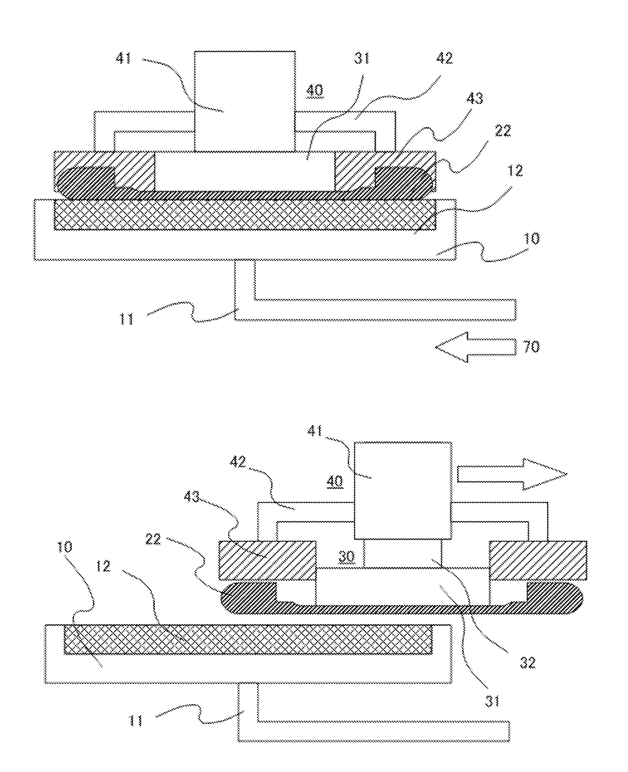
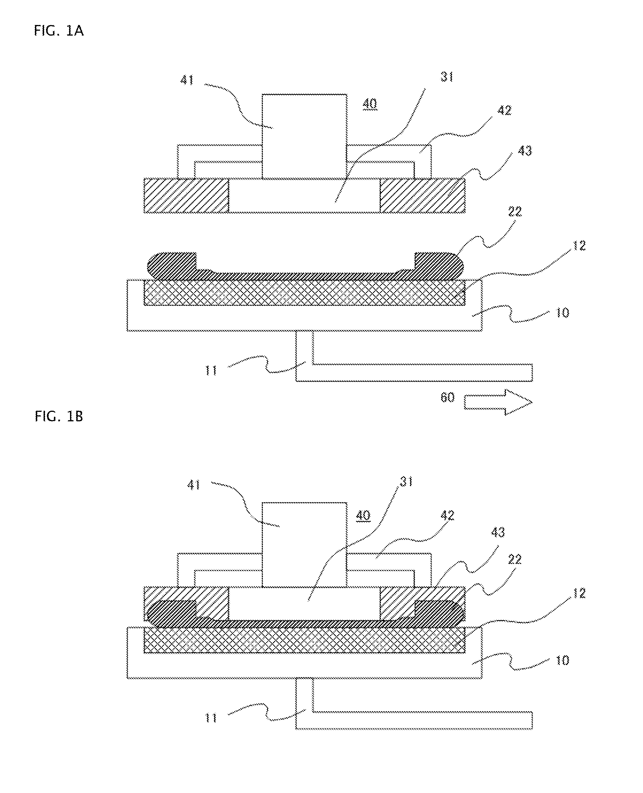
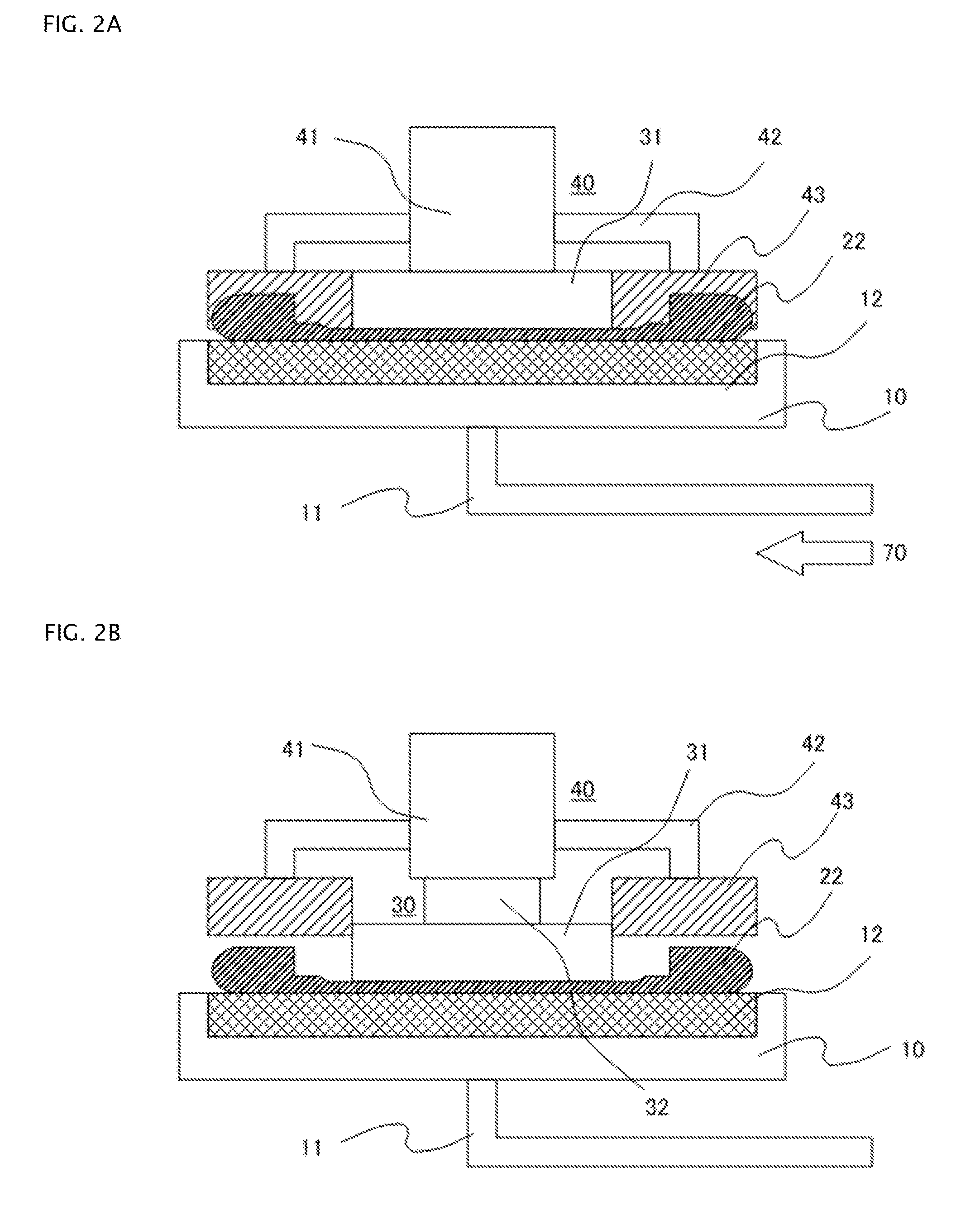
[0057]FIGS. 1A, 1B, FIGS. 2A, 2B, FIGS. 3A, 3B, FIGS. 4A, 4B, 4C, and FIGS. 5A, 5B illustrates the first embodiment according to the present invention. Of the figures, FIGS. 4A, 4B, and 4C are timing charts showing pressures on some parts in the embodiment.

[0058]FIG. 1A shows a wafer 22 attached by suction on the surface of an attachment plate 12 of a chuck table 10. The attachment plate 12 is made of a porous material and has a surface machined to be flat for attaching the wafer 22. The chuck table 10 is connected to a vacuum system (not depicted) through a supply and exhaust path 11. A negative pressure (indicated by the symbol 60) supplied by the vacuum system is transmitted to the surface of the attachment plate 12 and attracts the wafer 22 through vacuum suction. FIG. 1A shows the wafer 22 after completion of a grinding step as illustrated in FIGS. 12A through 12D, FIGS. 13A, 13B, and FIGS. 14A, 14B, and 14C.

[0059]The following describes a procedure of transferring the wafer 22...

second embodiment

[0085]The second embodiment according to the present invention will be described in the following with reference to FIGS. 7A, 7B, FIGS. 8A, 8B, FIGS. 9A, 9B, and FIGS. 10A, 10B, and 10C.

[0086]FIGS. 7A, 7B, FIGS. 8A, 8B, FIGS. 9A, 9B, and FIGS. 10A, 10B, and 10C illustrate the second aspect of embodiment according to the present invention. Of these figures, FIGS. 10A, 10B, and 10C are timing charts showing pressure at some parts in the device of the embodiment.

[0087]FIG. 7A shows a wafer 22 attached by suction on the surfaces of attachment plates 13 and 14 of a chuck table 10. The attachment plates 13 and 14 are made of a porous material and have a surface machined to be flat for attaching the wafer 22. The attachment plate 13 to attach the outer peripheral portion of the wafer 22 is made of a relatively high density porous material and has a structure that effectively transmits a negative pressure from a supply and exhaust path 11 to the attracted surface of the wafer 22. Because of...


PUM

PropertyMeasurementUnit
thicknessaaaaaaaaaa
thicknessaaaaaaaaaa
widthaaaaaaaaaa

Abstract

A method of transporting a semiconductor wafer having a ring-shaped stiffening portion can include the steps of pressing the semiconductor wafer from the back surface side to the front surface side thereof on a place different from a place at which the semiconductor wafer is to be held, the step of pressing the semiconductor wafer being conducted before holding the semiconductor wafer having the ring-shaped stiffening portion. The method can include releasing the attachment by suction of the front surface of the semiconductor wafer by supplying a positive pressure onto the chuck table, releasing pressing the semiconductor wafer from the back surface side to the front surface side thereof on the place different from the place at which the semiconductor wafer is to be held and picking up the semiconductor wafer having the ring-shaped stiffening portion from the chuck table while holding the semiconductor wafer.

Description

BACKGROUND OF THE INVENTION[0001]1. Field of the Invention[0002]Embodiments of the invention relate to methods and apparatuses for manufacturing a semiconductor device, and, in particular, to methods and apparatuses for manufacturing thin semiconductor devices such as power semiconductor devices used in power conversion devices.[0003]2. Description of the Related Art[0004]In power semiconductor devices represented by IGBTs (insulated gate bipolar transistors), methods are being developed to reduce the thickness of semiconductor substrates or wafers for producing semiconductor devices to achieve high performance of the devices. In addition, wafers with enlarged diameters are being developed to increase the number of power semiconductor elements that can be formed of a sheet of wafer, thereby reducing the costs of the semiconductor devices.[0005]The reduction in wafer thickness, however, in certain circumstances, may cause a break at the peripheral edge of the wafer resulting in chipp...

Claims


Application Information

Patent Timeline
Patent Type & Authority Patents(United States)
IPC IPC(8): B24B7/04
CPCH01L21/6838
Inventor TANAKA, YOKO
Owner FUJI ELECTRIC CO LTD
Learn More