

Method and apparatus for manufacturing a semiconductor device
a semiconductor device and manufacturing method technology, applied in the direction of grinding drives, manufacturing tools, grinding machine components, etc., can solve the problems of reducing mechanical strength, reducing the efficiency of manufacturing, affecting the quality of manufacturing, so as to prevent the wafer from chipping and cracking. , the effect of safe and sure picking up
- Summary
- Abstract
- Description
- Claims
- Application Information
AI Technical Summary
Benefits of technology
Problems solved by technology
Method used
Image

Examples
first embodiment
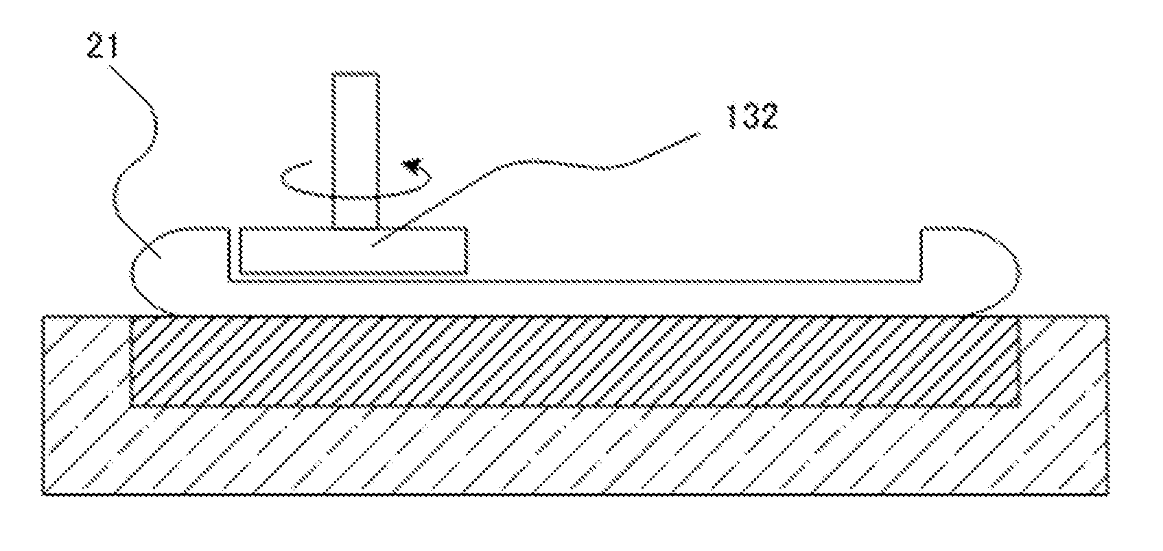
[0056]A wafer having a ring-shaped stiffening portion at the periphery of the wafer as shown in FIGS. 12A through 12D can be formed by a process as shown in FIGS. 13A, 13B, and FIGS. 14A, 14B, and 14C. Descriptions on the FIGS. 12A through 12D and FIGS. 13A, 13B, and FIGS. 14A, 14B, and 14C have been made in the foregoing and are not repeated here.
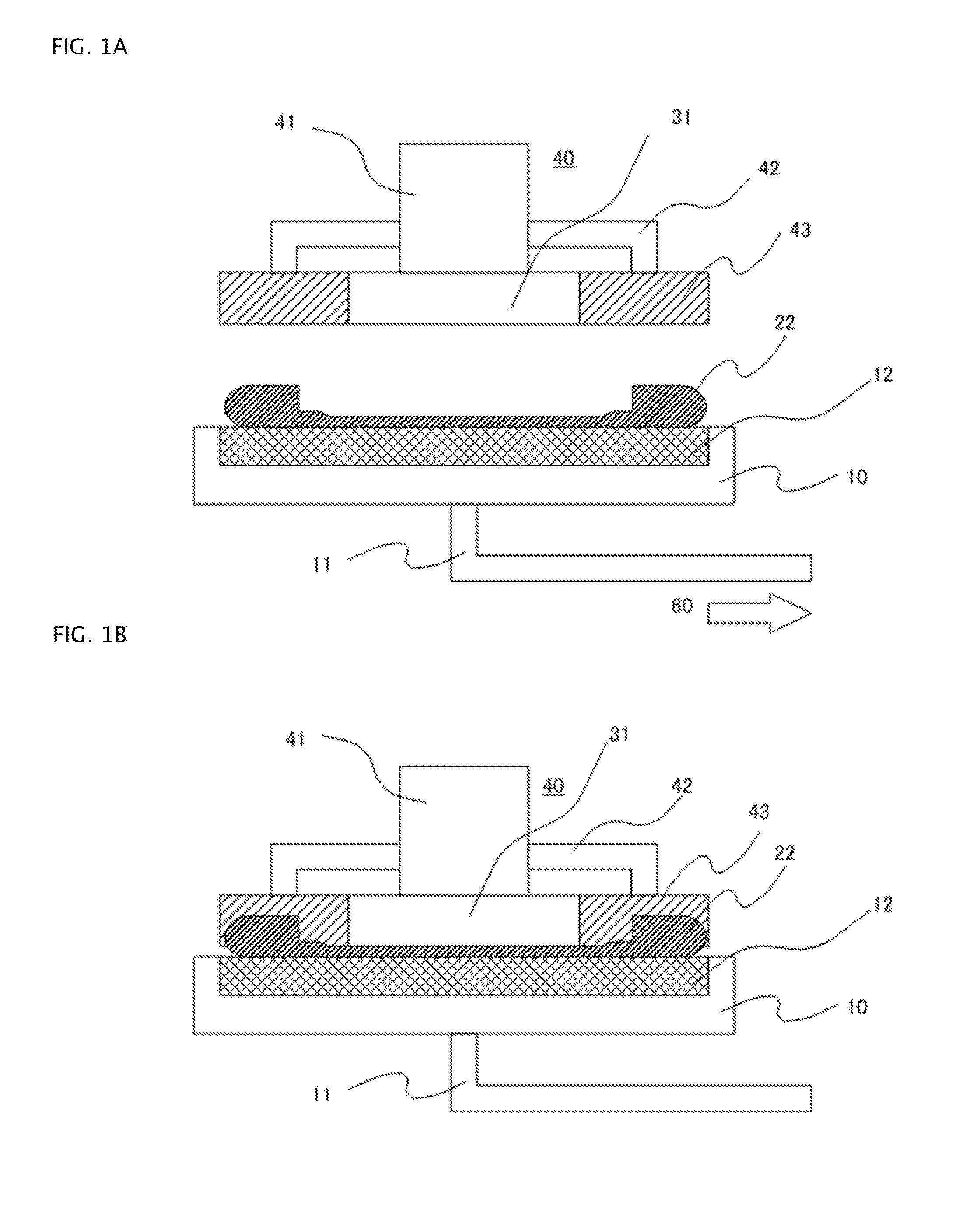
[0057]FIGS. 1A, 1B, FIGS. 2A, 2B, FIGS. 3A, 3B, FIGS. 4A, 4B, 4C, and FIGS. 5A, 5B illustrates the first embodiment according to the present invention. Of the figures, FIGS. 4A, 4B, and 4C are timing charts showing pressures on some parts in the embodiment.
[0058]FIG. 1A shows a wafer 22 attached by suction on the surface of an attachment plate 12 of a chuck table 10. The attachment plate 12 is made of a porous material and has a surface machined to be flat for attaching the wafer 22. The chuck table 10 is connected to a vacuum system (not depicted) through a supply and exhaust path 11. A negative pressure (indicated by the symbol 60) suppl...
second embodiment
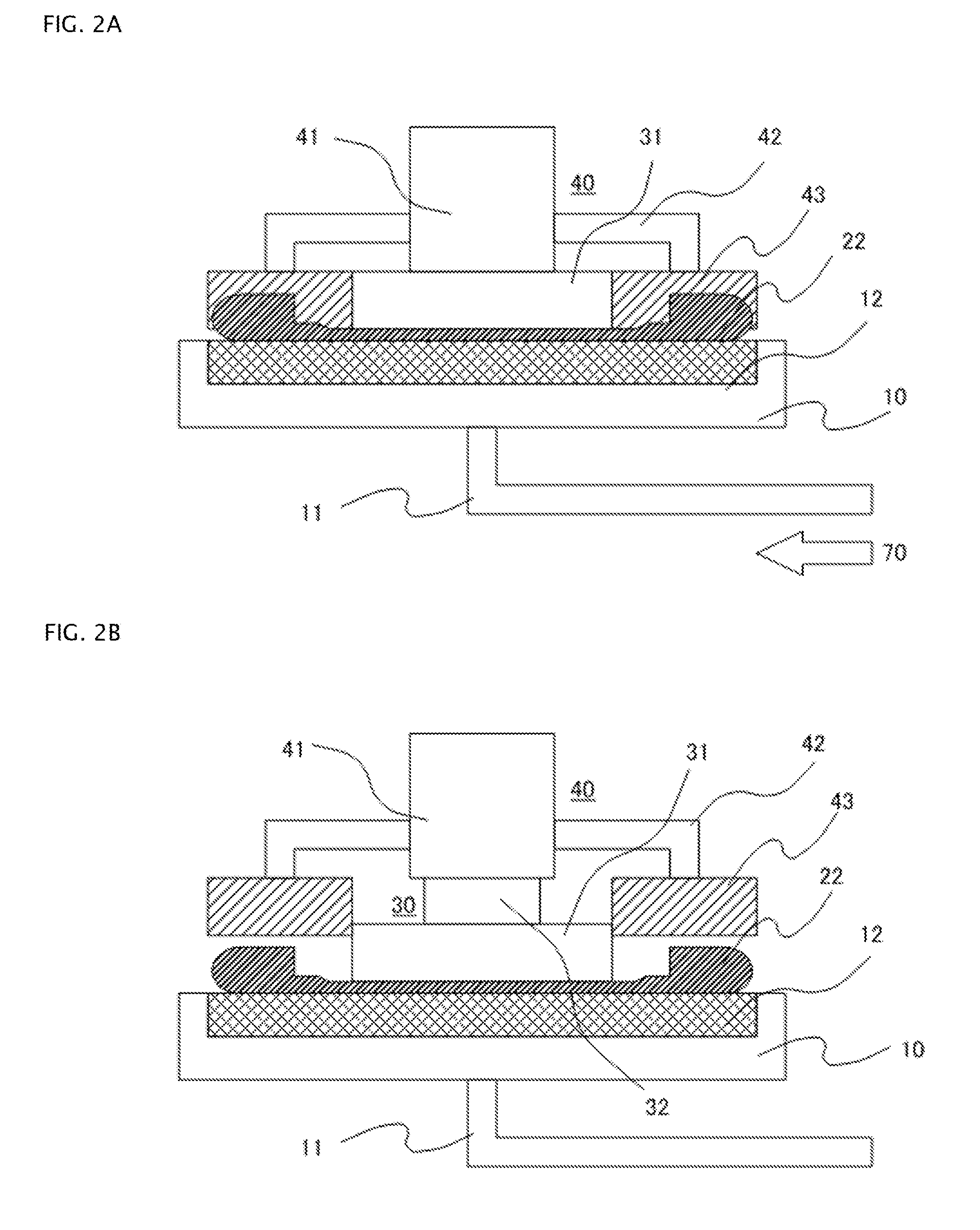
[0085]The second embodiment according to the present invention will be described in the following with reference to FIGS. 7A, 7B, FIGS. 8A, 8B, FIGS. 9A, 9B, and FIGS. 10A, 10B, and 10C.
[0086]FIGS. 7A, 7B, FIGS. 8A, 8B, FIGS. 9A, 9B, and FIGS. 10A, 10B, and 10C illustrate the second aspect of embodiment according to the present invention. Of these figures, FIGS. 10A, 10B, and 10C are timing charts showing pressure at some parts in the device of the embodiment.
[0087]FIG. 7A shows a wafer 22 attached by suction on the surfaces of attachment plates 13 and 14 of a chuck table 10. The attachment plates 13 and 14 are made of a porous material and have a surface machined to be flat for attaching the wafer 22. The attachment plate 13 to attach the outer peripheral portion of the wafer 22 is made of a relatively high density porous material and has a structure that effectively transmits a negative pressure from a supply and exhaust path 11 to the attracted surface of the wafer 22. Because of...
PUM
| Property | Measurement | Unit |
|---|---|---|
| thickness | aaaaa | aaaaa |
| thickness | aaaaa | aaaaa |
| width | aaaaa | aaaaa |
Abstract
Description
Claims
Application Information