Graphene photodetector

a graphene-based photodetector and photodetector technology, applied in the direction of photovoltaic energy generation, electrical apparatus, semiconductor devices, etc., can solve the problems of carrier lifetime and formation of compact optoelectronic devices based on graphene, and achieve the effects of enhancing the photoresponse of graphene-based photodetectors, minimizing travel distances, and high efficiency

Active Publication Date: 2014-12-02
INT BUSINESS MASCH CORP
View PDF8 Cites 13 Cited by
  • Summary
  • Abstract
  • Description
  • Claims
  • Application Information

AI Technical Summary

Benefits of technology

[0003]A photodetector based on a graphene layer can provide high efficiency by geometrically arranging a plurality of electrodes to minimize travel distances for charge carriers generated by photons. The photodetector utilizes both photovoltaic effects and photo-thermo-electric (PTE) effects to enhance the photoresponse of a graphene-based photodetector.
[0005]Multiple p-n junctions are formed in a graphene layer such that the p-n junctions are located within multiple pairs of metallic fingers of different types. The response of the photodetector of the present invention is due to the photovoltaic and photothermoelectric effect at the p-n junctions in the graphene layer. These two effects produces a photocurrent in the same direction. The three effects result in electrical currents that flow along a same direction, thereby proving a greater photocurrent than a component of the electrical current due to the photovoltaic effect only. The location of the p-n junctions can be optimized by adjusting the magnitude of electrical bias applied to the buried electrodes. The lengths of the first and second upper electrodes and the buried electrodes can also be optimized to enhance the photoresponse of the device. Further, the device of the present invention can be integrated into standard semiconductor manufacturing schemes to provide low cost electromagnetic radiation detectors.

Problems solved by technology

Despite the superior performance potential of a graphene relative to silicon and group III-V semiconductor compounds in terms of such properties, formation of a compact optoelectronic device based on a graphene is a significant challenge because coupling between electromagnetic radiation and charge carriers of the graphene layer is relatively weak and because the charge carrier lifetime in a graphene layer is relatively short.

Method used


Image

  • Graphene photodetector
  • Graphene photodetector
  • Graphene photodetector

Examples


Embodiment Construction

[0014]As stated above, the present invention relates to a photodetector employing a sheet of graphene and methods of manufacturing and operating the same. Aspects of the present invention are now described in detail with accompanying figures. It is noted that like reference numerals refer to like elements across different embodiments. As used herein, ordinals such as “first” and “second” are employed merely to distinguish similar elements, and different ordinals may be employed to designate a same element in the specification and / or claims.

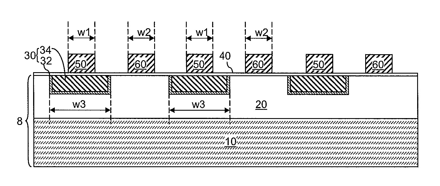
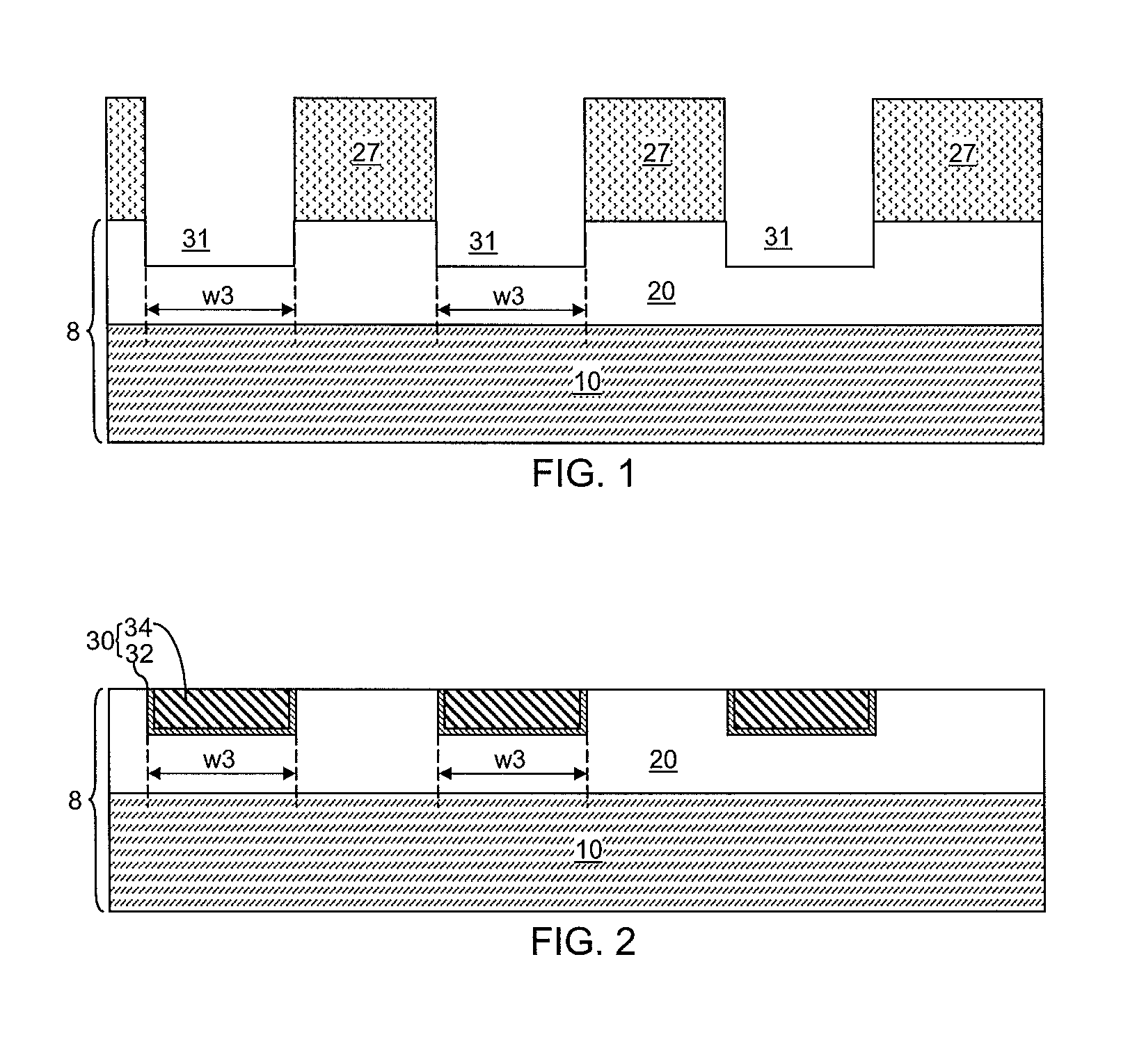
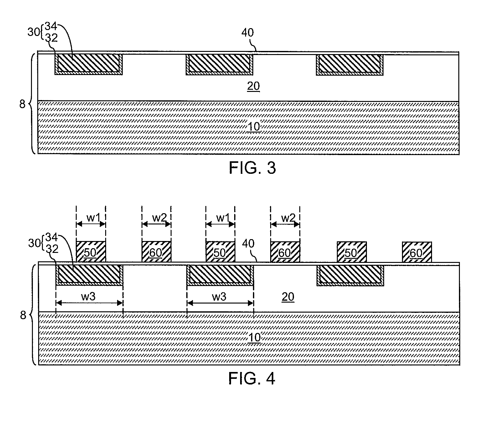
[0015]Referring to FIG. 1, an exemplary structure according to an embodiment of the present invention includes a substrate 8, which includes a stack of a handle substrate 10 and an insulator layer 20. The handle substrate 10 can include a semiconductor material, a dielectric material, or a conductive material, and provides mechanical support to the insulator layer 20 and the structures to be formed thereupon. The insulator layer 20 includes a diel...


PUM


Abstract

A set of buried electrodes are embedded in a dielectric material layer, and a graphene layer having a doping of a first conductivity type are formed thereupon. A first upper electrode is formed over a center portion of each buried electrode. Second upper electrodes are formed in regions that do not overlie the buried electrodes. A bias voltage is applied to the set of buried electrodes to form a charged region including minority charge carriers over each of the buried electrodes, and to form a p-n junction around each portion of the graphene layer overlying a buried electrode. Charge carriers generated at the p-n junctions are collected by the first upper electrodes and the second upper electrodes, and are subsequently measured by a current measurement device or a voltage measurement device.

Description

BACKGROUND[0001]The present invention relates to an optoelectronic device, and particularly to a photodetector employing a sheet of graphene and methods of manufacturing and operating the same.[0002]Two-dimensional carbon lattice structures include sp2-bonded carbon atoms that are densely packed in a hexagonal lattice structure. If the two-dimensional carbon lattice structure is topologically planar, the two-dimensional carbon lattice structure constitutes a graphene layer. A graphene layer absorbs and emits light across the entire range of the electromagnetic spectrum, and sustains high electrical current densities and extreme temperatures. Despite the superior performance potential of a graphene relative to silicon and group III-V semiconductor compounds in terms of such properties, formation of a compact optoelectronic device based on a graphene is a significant challenge because coupling between electromagnetic radiation and charge carriers of the graphene layer is relatively we...

Claims


Application Information

Patent Timeline
Patent Type & Authority Patents(United States)
IPC IPC(8): H01L27/14H01L31/18H01L31/028H01L31/0224
CPCH01L31/022408H01L31/028H01L31/1804H01L31/0224H01L31/09H01L31/108Y02E10/547
Inventor AVOURIS, PHAEDONLOW, TONY A.XIA, FENGNIAN
Owner INT BUSINESS MASCH CORP
Why Eureka
Try Eureka