Check patentability & draft patents in minutes with Patsnap Eureka AI!

III-nitride transistor with source-connected heat spreading plate

a technology of iiinitride and heat spreading plate, which is applied in the direction of semiconductor/solid-state device details, semiconductor devices, electrical apparatus, etc., can solve the problems of substrate backgating problem, substrate backgating problem, and loss of control on the back side voltage, etc., and achieve the effect of reducing backgating phenomena

Active Publication Date: 2014-12-23
INTERUNIVERSITAIR MICRO ELECTRONICS CENT (IMEC VZW)
View PDF5 Cites 0 Cited by
  • Summary
  • Abstract
  • Description
  • Claims
  • Application Information

AI Technical Summary

Benefits of technology

This solution effectively increases breakdown voltage, reduces buffer leakage current, and improves thermal dissipation without increasing buffer thickness, addressing the limitations of Si substrate removal.

Problems solved by technology

The above-described Si removal may prove undesirable for at least two reasons.
First, a substrate backgating problem may arise.
In this case, any control on the back side voltage is lost, and undesirable back side gating can reduce the on-state current and increase the on-resistance.
If a Si substrate is present, it is possible to connect it to the source, but this decreases the breakdown voltage.
Second, a thermal dissipation problem may arise.
Therefore, when the Si substrate is removed, heat dissipation can be an issue.

Method used


Image

  • III-nitride transistor with source-connected heat spreading plate
  • III-nitride transistor with source-connected heat spreading plate
  • III-nitride transistor with source-connected heat spreading plate

Examples


Embodiment Construction

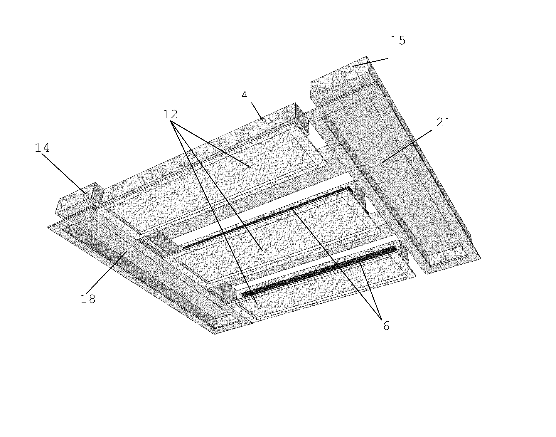
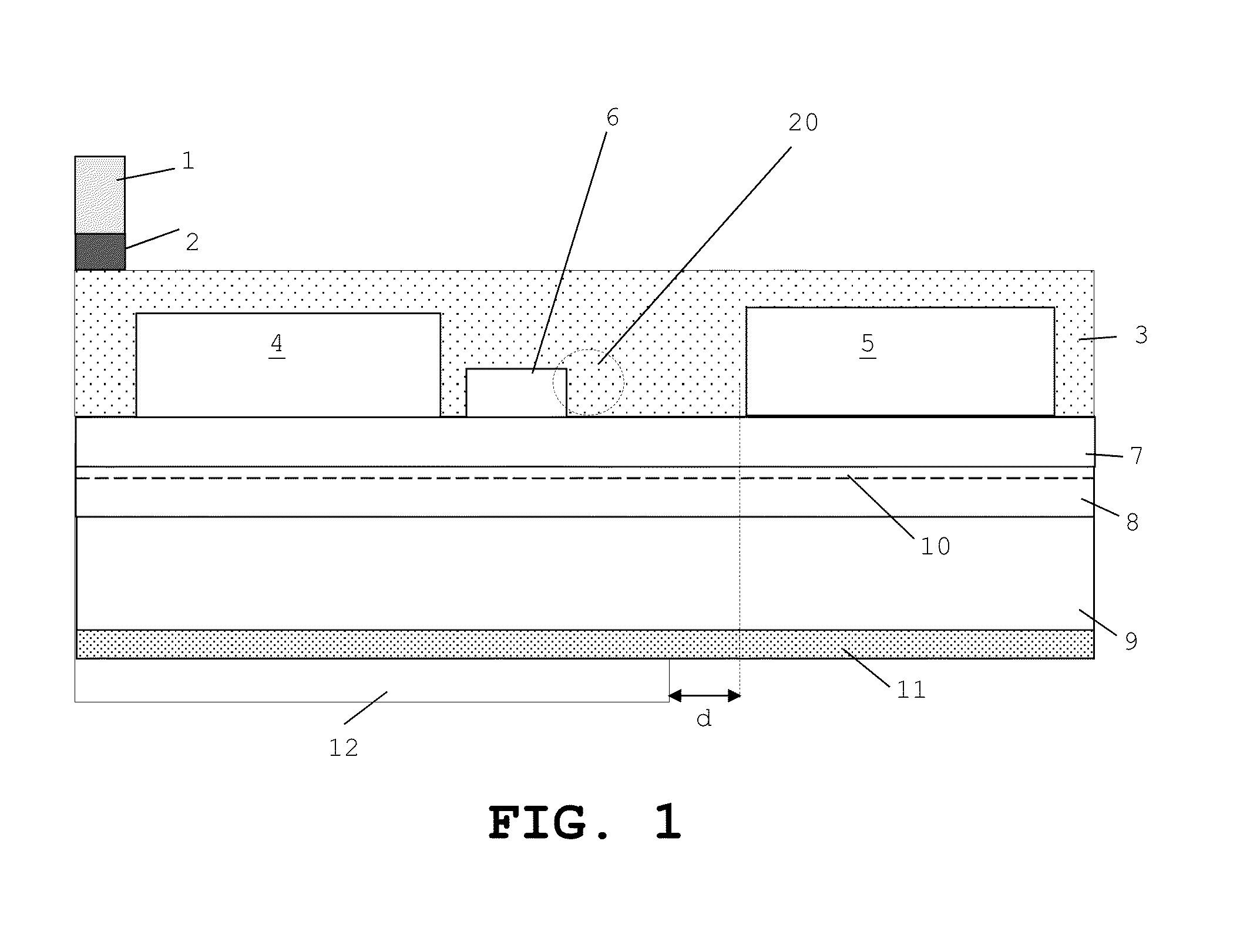
[0016]FIGS. 1 and 2 each illustrate a possible embodiment of a transistor according to the disclosure. The figures may be seen as cross-sections of a single transistor or of a portion of a high power High Electron Mobility Transistor (HEMT) device structure with multiple interlocking source and drain fingers, connected to contact pads, as illustrated in FIG. 3. As shown in FIG. 3, the HEMT device structure may include an active area 50. The active area may be, for example, the area in which actual currents take place through the transistor's channel when the transistor is conducting. The active area may be distinguished from, for example, the source and drain contact pads 14, 15. The views shown in FIGS. 1 and 2 may be seen as cross-sections taken in the active area 50, along the line indicated as ‘A’ in FIG. 3. Nevertheless, the disclosure is not limited to a particular transistor design.

[0017]As shown in FIG. 1, an example device may include a carrier substrate 1, a bonding layer ...


PUM


Abstract

Disclosed are semiconductor devices and methods for manufacturing them. An example device may include a III-nitride stack having a front side surface and a back side surface. The III-nitride stack may be formed of at least a first layer and a second layer, between which a heterojunction may be formed, such that a two-dimensional electron gas layer is formed in the second layer. A source electrode, a drain electrode, and a gate electrode positioned between the source and drain electrodes may be formed on the front side surface, and an insulation layer may be formed over the electrodes on the front side surface. A carrier substrate may be attached to the insulation layer. An electrically conductive back plate may be formed on the back side surface. The back plate may directly face the source electrode and the gate electrode, but not the drain electrode.

Description

CROSS-REFERENCE TO RELATED APPLICATION[0001]The present application claims priority to European Patent Application Serial No. 12196215.3 filed Dec. 10, 2012, the contents of which are hereby incorporated by reference.BACKGROUND[0002]Gallium Nitride-on-Silicon (GaN-on-Si) power devices are affected by a parasitic conductive layer at an interface between the Si and the III / Nitride stack, which increases the buffer leakage current and reduces the breakdown voltage. This detrimental conductive path can be interrupted by removing the Si substrate, globally over the entire wafer, as described in, for example, “Silicon Substrate Removal of GaN DHFETs for enhanced (>1100V) Breakdown voltage,” P. Srivastava et al., IEEE Electron Device Letters 31 (8), pp 851-853, 2010. Alternatively, the detrimental conductive path can be interrupted by removing the Si substrate selectively at specific locations, as described in, for example, “Si trench around drain (STAD) technology of GaN-DHFETs on Si s...

Claims


Application Information

Patent Timeline
Patent Type & Authority Patents(United States)
IPC IPC(8): H01L29/20H01L21/308H01L23/482H01L21/00H01L29/417H01L23/34H01L29/66H01L21/283H01L21/28H01L29/778H01L21/48
CPCH01L29/2003H01L29/7786H01L23/4824H01L21/308H01L21/4814H01L21/283H01L2924/0002H01L29/778H01L29/41758H01L21/28247H01L29/66431H01L29/4175H01L2924/00
Inventor LENCI, SYLVIADECOUTERE, STEFAAN
Owner INTERUNIVERSITAIR MICRO ELECTRONICS CENT (IMEC VZW)
Features
  • R&D
  • Intellectual Property
  • Life Sciences
  • Materials
  • Tech Scout
  • Unparalleled Data Quality
  • Higher Quality Content
  • 60% Fewer Hallucinations
Learn More