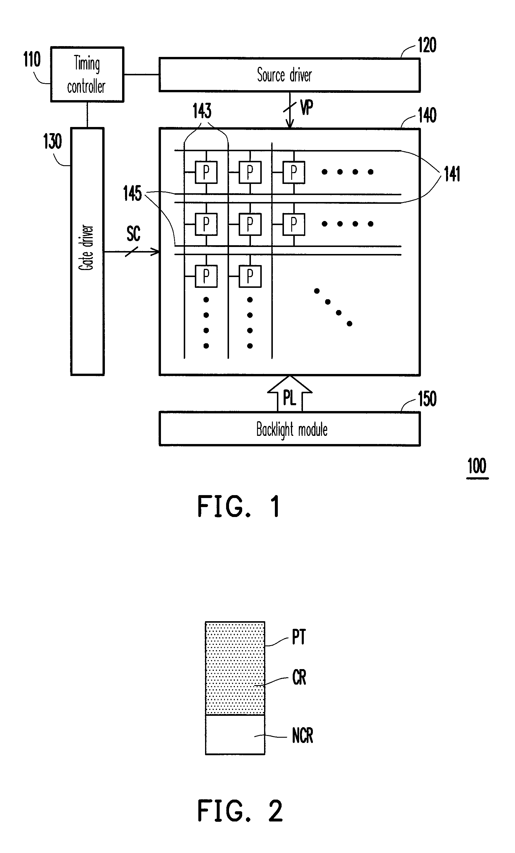
Pixel structure
a liquid crystal display and pixel technology, applied in the field of pixel structure, can solve the problems of cost and space consumption of purchasing and accommodating display devices
- Summary
- Abstract
- Description
- Claims
- Application Information
AI Technical Summary
Benefits of technology
Problems solved by technology
Method used
Image

Examples
first embodiment
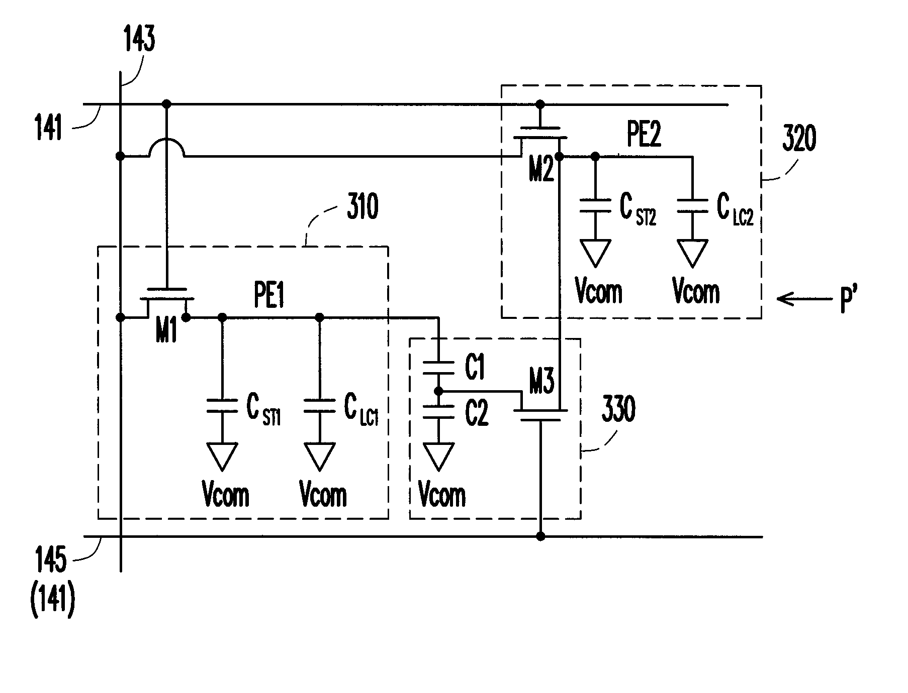
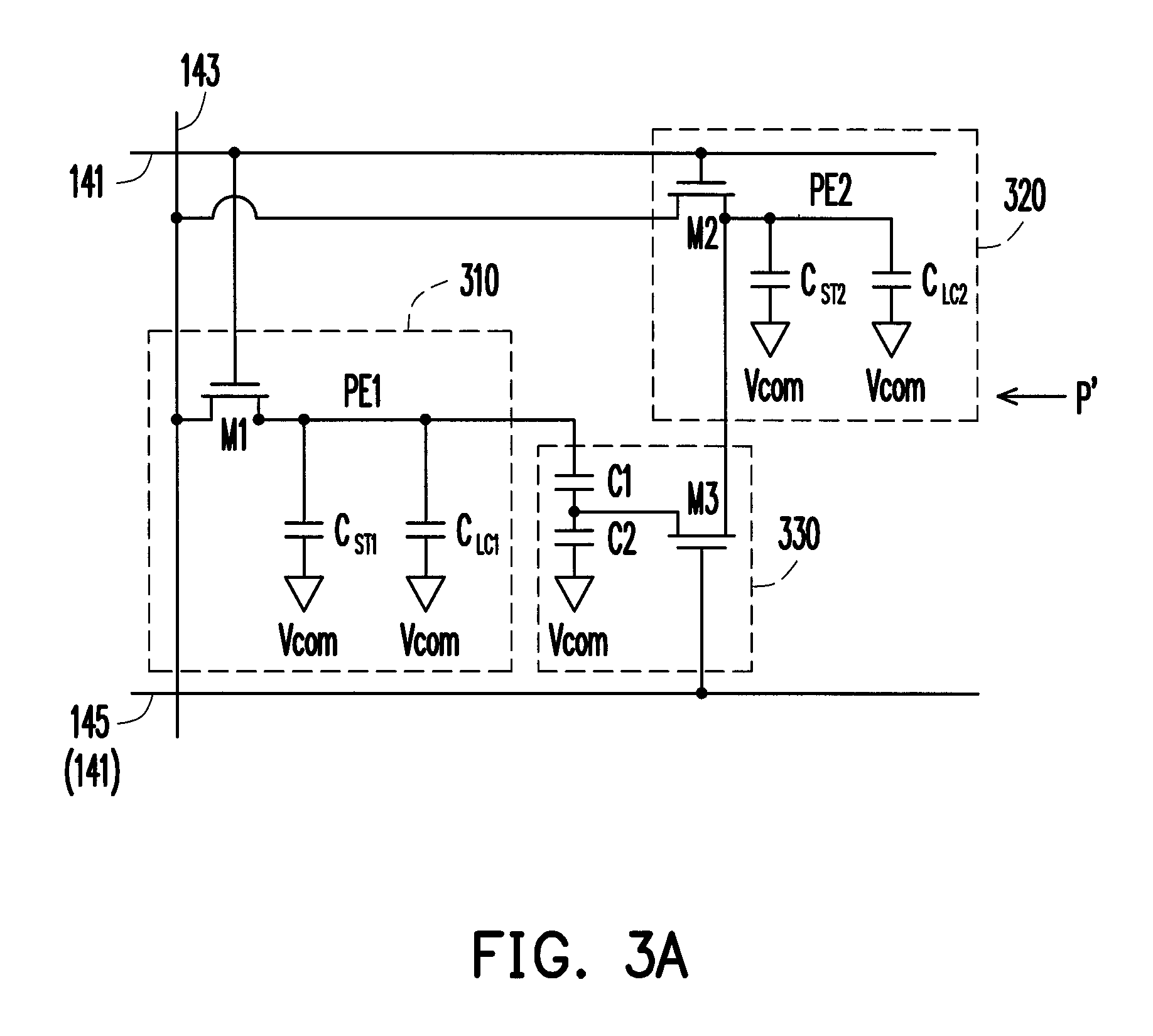
[0040]FIG. 3A is a schematic diagram of a circuit structure of the pixel P in FIG. 1 according to the present invention. Referring to FIG. 3A, in this embodiment, the pixel structure P′ includes a first pixel unit 310, a second pixel unit 320 and a discharge unit 330. The color resistant region CR in FIG. 2 is configured corresponding to the first pixel unit 310 and the non-color resistant region NCR in FIG. 2 is configured corresponding to the second pixel unit 320. The pixel structure P′ of this embodiment is adapted for a normal black display panel.
[0041]The first pixel unit 310 includes a first active device (here, for example TFT M1), a first pixel electrode PE1, a first storage capacitor CST1 and a first liquid crystal capacitor CLC1. A gate of the TFT M1 is electrically connected to the scan line 141, a drain of the TFT M1 is electrically connected to the data line 143 and a source of the TFT M1 is electrically connected to the first pixel electrode PE1. The first storage cap...
second embodiment
[0055]FIG. 4A is a schematic diagram of a circuit structure of a pixel P in FIG. 1 according to the present invention. Referring to FIG. 3A and FIG. 4A, the difference between the pixels P′ and P″ is that the discharge unit 410 is electrically connect to the pixels P″. The discharge unit 410 includes a second switch (here, for example, the TFT M4). The source (corresponding to the third end) of the TFT M4 is electrically connected to the common voltage Vcom, the drain (corresponding to the fourth end) of the TFT M4 is electrically connected to the second pixel electrode PE2 and a gate (corresponding to the second control end) of the TFT M4 is electrically connected to the driving line 145.
[0056]Referring to FIG. 1, FIG. 2 and FIG. 4A, when the TFT M4 is controlled by the signal (corresponding to the driving signal) transferred by the driving line 145 to be conducted, the voltage of the second pixel electrode PE2 is equal to the common voltage Vcom, that is, the voltage of the second...
third embodiment
[0065]FIG. 5A is a schematic diagram of a circuit structure of a pixel P in FIG. 1 according to the present invention. Referring to FIG. 3A and FIG. 5A, the difference between the pixels P′ and P′″ is that the discharge unit 510 is electrically connect to the pixels P′″. The discharge unit 510 is further electrically connected to the scan line 141. The discharge unit 510 includes a third switch (here, for example, the TFT M4) and a fourth switch (here, for example, the TFT M5). The source (corresponding to the fifth end) of the TFT M4 is electrically connected to the common voltage Vcom, the drain (corresponding to the sixth end) of the TFT M4 is electrically connected to the source (corresponding to the seventh end) of the TFT M5 and the gate (corresponding to the third control end) of the TFT M4 is electrically connected to the scan line 141. The drain (corresponding to the eighth end) of the TFT M5 is electrically connected to the second pixel electrode PE2, the gate (correspondi...
PUM
| Property | Measurement | Unit |
|---|---|---|
| transparent | aaaaa | aaaaa |
| light transmittance | aaaaa | aaaaa |
| light transmittance | aaaaa | aaaaa |
Abstract
Description
Claims
Application Information
 - R&D
- Intellectual Property
- Life Sciences
- Materials
- Tech Scout
- Unparalleled Data Quality
- Higher Quality Content
- 60% Fewer Hallucinations
Browse by: Latest US Patents, China's latest patents, Technical Efficacy Thesaurus, Application Domain, Technology Topic, Popular Technical Reports.
© 2025 PatSnap. All rights reserved.Legal|Privacy policy|Modern Slavery Act Transparency Statement|Sitemap|About US| Contact US: help@patsnap.com