Supercharge Your Innovation With Domain-Expert AI Agents!

Light emitting diode

a technology of light-emitting diodes and diodes, which is applied in the direction of basic electric elements, electrical equipment, semiconductor devices, etc., can solve the problem of low light-extraction efficiency of leds

Active Publication Date: 2015-02-03
TSINGHUA UNIV +1
View PDF8 Cites 0 Cited by
  • Summary
  • Abstract
  • Description
  • Claims
  • Application Information

AI Technical Summary

Benefits of technology

The implementation of a three-dimensional nano-structure array increases light extraction efficiency by approximately four times compared to LEDs without such structures, effectively addressing the issue of internal reflection and improving overall light output.

Problems solved by technology

However, the light-extraction efficiency of LEDs is low because typical semiconductor materials have a higher refraction index than that of air.

Method used


Image

  • Light emitting diode
  • Light emitting diode
  • Light emitting diode

Examples


Embodiment Construction

[0019]The disclosure is illustrated by way of example and not by way of limitation in the figures of the accompanying drawings in which like references indicate similar elements. It should be noted that references to “an” or “one” embodiment in this disclosure are not necessarily to the same embodiment, and such references mean “at least one”.

[0020]References will be made to the drawings to describe, various embodiments of the present LED.

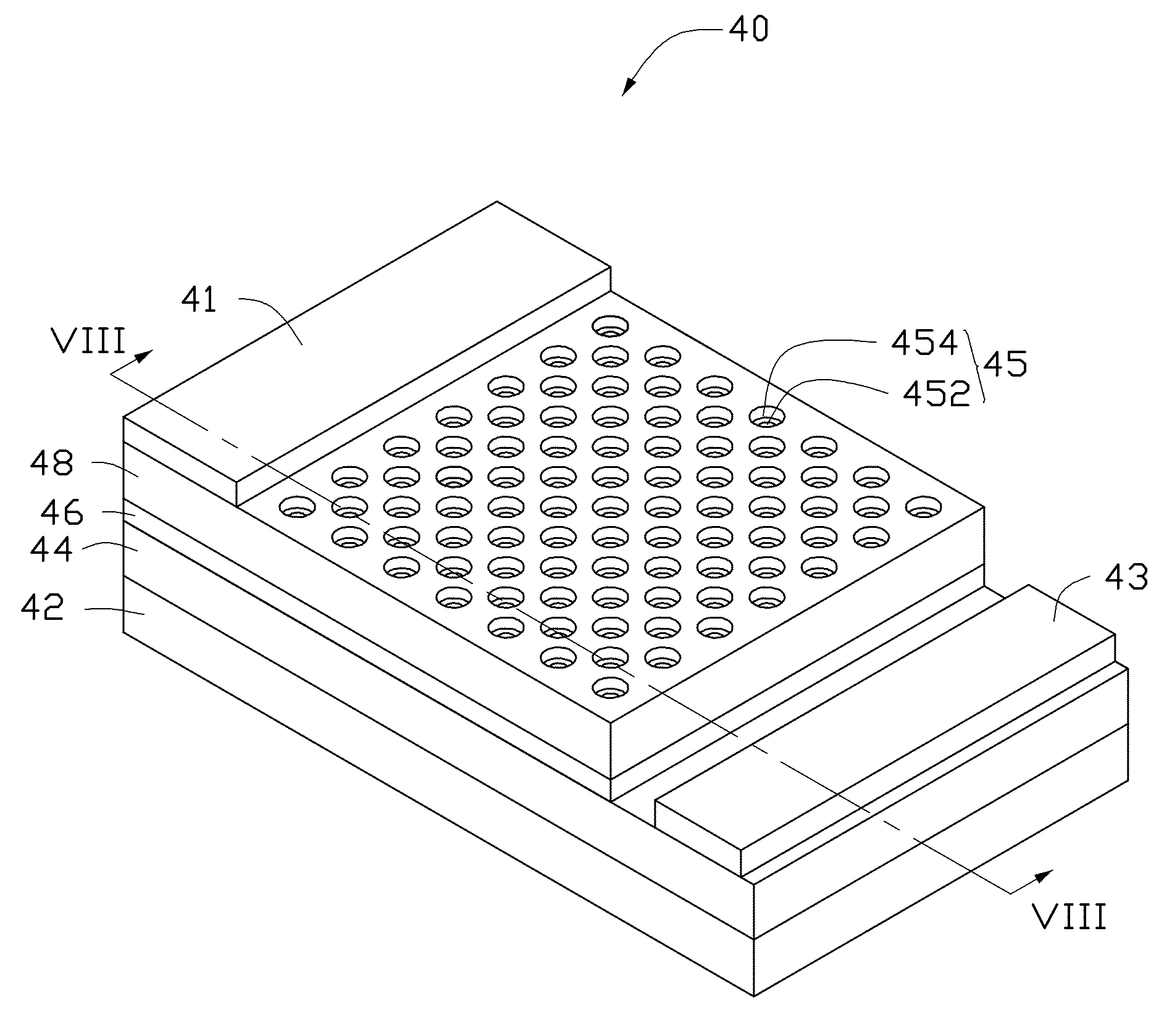
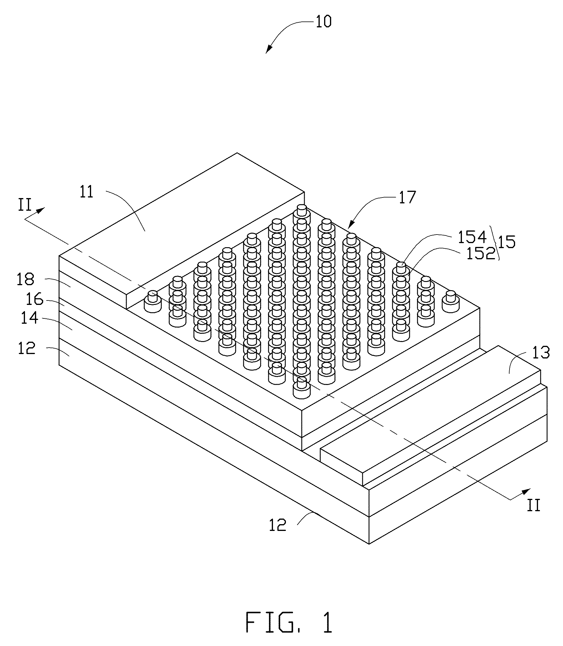
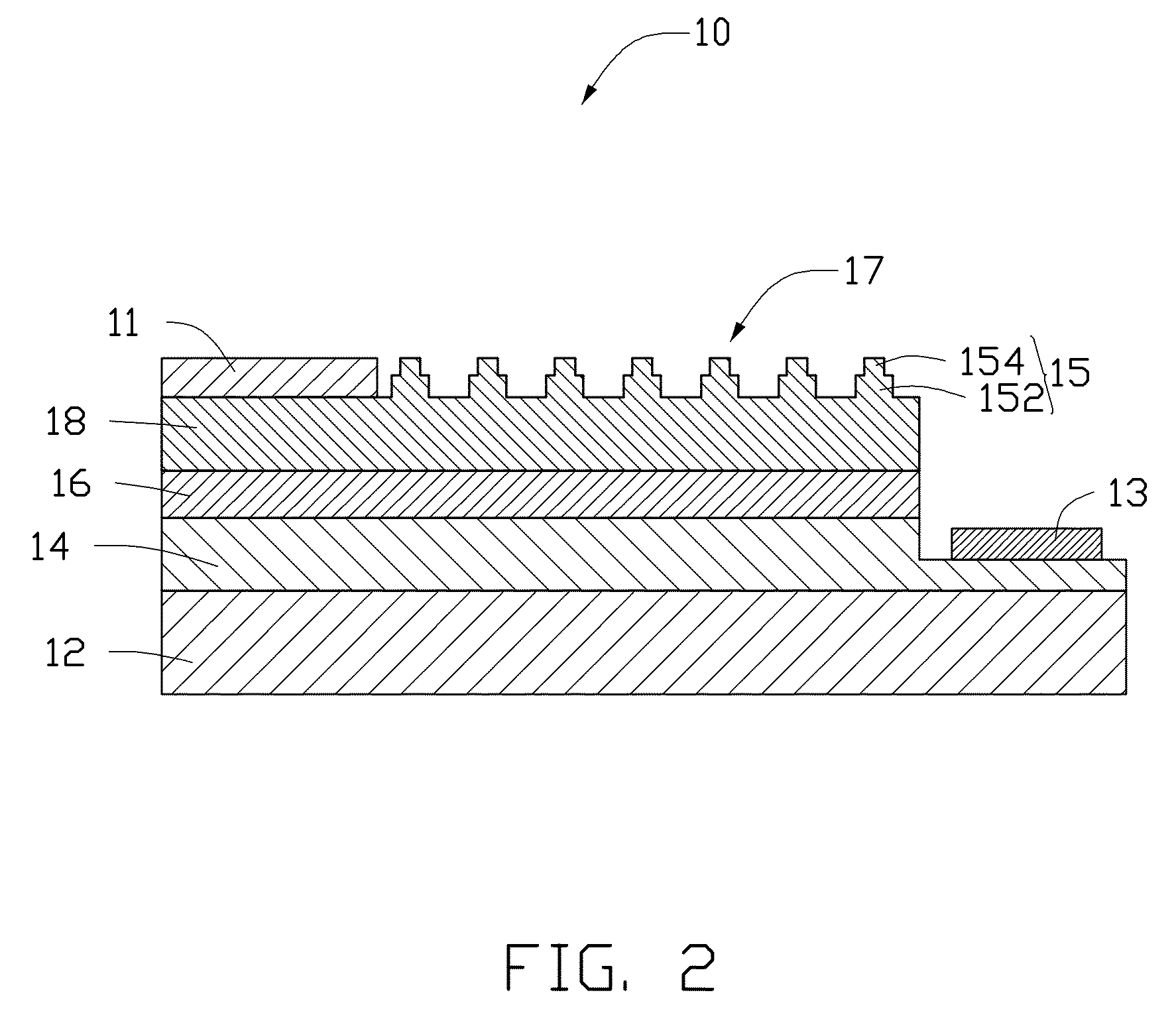
[0021]Referring to FIGS. 1 to 2, an embodiment of an LED 10 includes a substrate 12, a first semiconductor layer 14, an active layer 16, a second semiconductor layer 18, a first electrode 13, a second electrode 11, and a three-dimensional nano-structure array 17.

[0022]The first semiconductor layer 14, the active layer 16, and the second semiconductor layer 18 are orderly stacked on a top surface of the substrate 12. The first electrode 13 is electrically connected to the first semiconductor layer 14. The second electrode 11 is electrically connecte...


PUM


Abstract

A light emitting diode includes a substrate, a first semiconductor layer, an active layer, a second semiconductor layer, a first electrode, and a second electrode. The first semiconductor layer, the active layer, and the second semiconductor layer are orderly stacked on the substrate. The second semiconductor layer is covered with stepped three-dimensional nano-structures in a particular shape, which act to reabsorb wide-angle incident light and re-emit the light at narrower angles of incidence, to increase the light-giving properties of the light emitting diode.

Description

CROSS-REFERENCE TO RELATED APPLICATIONS[0001]This application is a continuation of U.S. patent application Ser. No. 12 / 970,234, filed on Dec. 16, 2010, entitled, “LIGHT EMITTING DIODE,” which claims all benefits accruing under 35 U.S.C. §119 from China Patent Application No. 201010192156.6, filed on Jun. 4, 2010 in the China Intellectual Property Office. The disclosures of the above-identified applications are incorporated herein by reference.BACKGROUND[0002]1. Technical Field[0003]The present disclosure relates to a light emitting diode (LED).[0004]2. Description of Related Art[0005]Highly efficient LEDs made with GaN-based semiconductors have become widely used in different technologies, such as in display devices, large electronic bill boards, street lights, car lights, and other illumination applications. LEDs are environmentally friendly, and have a long working life and low power consumption.[0006]A conventional LED commonly includes an N-type semiconductor layer, a P-type sem...

Claims


Application Information

Patent Timeline
Patent Type & Authority Patents(United States)
IPC IPC(8): H01L27/15H01L33/02H01L33/20
CPCH01L33/02H01L33/20H01L2933/0083
Inventor ZHU, ZHEN-DONGLI, QUN-QINGFAN, SHOU-SHAN
Owner TSINGHUA UNIV
Features
  • R&D
  • Intellectual Property
  • Life Sciences
  • Materials
  • Tech Scout
  • Unparalleled Data Quality
  • Higher Quality Content
  • 60% Fewer Hallucinations
Learn More