Electrical interconnect assembly

a technology of electrical interconnection and assembly, which is applied in the direction of electrically conductive connections, coupling device connections, measurement instrument housings, etc., can solve the problems of damage to the ic terminal during use and premature wear of the test terminal, so as to enhance the rigidity and co-planarity of the test contact, reduce vibration, and avoid the effect of vibration generated during us

Active Publication Date: 2015-02-10
JF MICROTECH
View PDF8 Cites 6 Cited by
  • Summary
  • Abstract
  • Description
  • Claims
  • Application Information

AI Technical Summary

Benefits of technology

[0010]In one embodiment, the head receiving portion restricts the test contact from moving laterally relative to a vertical plane intersecting the test terminal. In another embodiment, the head receiving portion restricts the test contact from moving vertically relative to the vertical plane intersecting the test terminal. That is, the retention of the first resiliently biasing member reduces vibration and enhances stability, rigidity and co-planarity of the test contact, in particular, during use.
[0011]In one embodiment, the first resiliently biasing member (e.g. top elastomer) is located vertically under the first electrical contacting portion (e.g. direct contact area) to absorb the force exerted on the test contact (e.g. test pin) during use. The top elastomer may also be pre-tensioned and is held in place by the head receiving portion of the test pin so that during use the pin only moves vertically downward relative to a vertical plane intersecting the test pin. Thus, by holding the pin in this manner, the test assembly avoids vibration generated during use and only provides a small indent mark on the test terminal rather than a long scratching mark or wiping. This motion also reduces pre-mature wearing of the IC terminals (e.g. contact pins) and improves their lifespan and test yield.
[0012]In one embodiment, the head receiving portion exerts a clamping force on the first resiliently biasing member to retain the test contact to the first resiliently biasing member. The head receiving portion may be at least partially circular. In an example of the test contact in use, the test contact retains the first resiliently biasing member to provide better alignment of the test contact with the corresponding IC terminal of an IC device being tested. The test contact thus minimizes its lateral movement during use and minimizes wear of the corresponding IC terminal (e.g. by scratching).
[0015]With this embodiment, the profile comprises a curved surface arranged such that during use rotation of the test contact effects regulation of the contact pressure between the test contact and the test terminal. Also, in an arrangement, the curved surface effects rotational movement of the test contact during use (e.g. a see-saw movement). In an example, the test contact minimizes wear from, for example, indenting the test terminals and the supporting load-board when used. Thus, in use, force is applied on the test contact which is distributed to the first resiliently biasing member acting as a vibration dampener and force dissipater. The test contact is moved down vertically so that its second electrical contacting portion (e.g. load-board contact radius) acts as a fulcrum (e.g. contact surface pivot point) which distributes force to the second resiliently biasing member (e.g. rear elastomer). In an arrangement, the rear elastomer is also pre-tensioned and the foot receiving portion retains the rear elastomer to the test contact to minimize vibration. In this case, the second biasing member also acts as counter force generator and a force dissipater to protect the load-board against wear or damage whilst maintaining contact with the load-board. Also, the profile of the test contact enables, after force is applied to the top of the test contact, the contact surface to contact the load-board without excessive pressure by diverting away some of the force with a sliding action / motion towards the second resiliently biasing member.
[0026]In an embodiment, the second resiliently biasing member prevents the test contacts from contacting the housing, in particular the corresponding contact sockets, with excessive force. Thus, in the embodiment, the second resiliently biasing member provides safety for the sockets and prevents the test contacts from over travelling their home position in their respective sockets by acting like a vertical spring loaded pin. The second biasing member also decelerates force applied to the test contacts, during testing, and pushes the test contacts back to their home position without excessive stress on the load-board to prolong load-board life and to improve test yield.
[0028]In this embodiment, the contact socket may also comprise a stop to restrict rotation of the test contact. Each contact socket and stop further improves co-planarity of the test contacts to minimize wear of the IC terminals.

Problems solved by technology

The test contacts in this arrangement, however, can transfer excessive force to the test terminal resulting in premature wear of the test terminal and can damage the IC terminal during use.

Method used


Image

  • Electrical interconnect assembly
  • Electrical interconnect assembly
  • Electrical interconnect assembly

Examples


Embodiment Construction

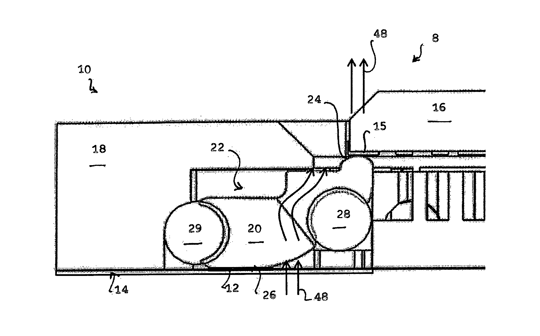
[0040]Referring to FIG. 1, a test system 8 is shown for testing IC devices. The test system 8 is of a type including an electrical interconnect assembly 10 according to an embodiment of the present invention for forming an electrical connection between test terminals 12 of a test assembly 14 and IC terminals 15 of an IC device 16 desired to be tested. The test terminals 12 are located on a load-board of the test assembly 14.

[0041]The test assembly 14 is arranged to carry out a series of tests on an IC device 16 connected to the test assembly 14 through the interconnect assembly 10, for example by applying defined signals to the test terminals 12, monitoring response signals and comparing the response signals to reference responses.

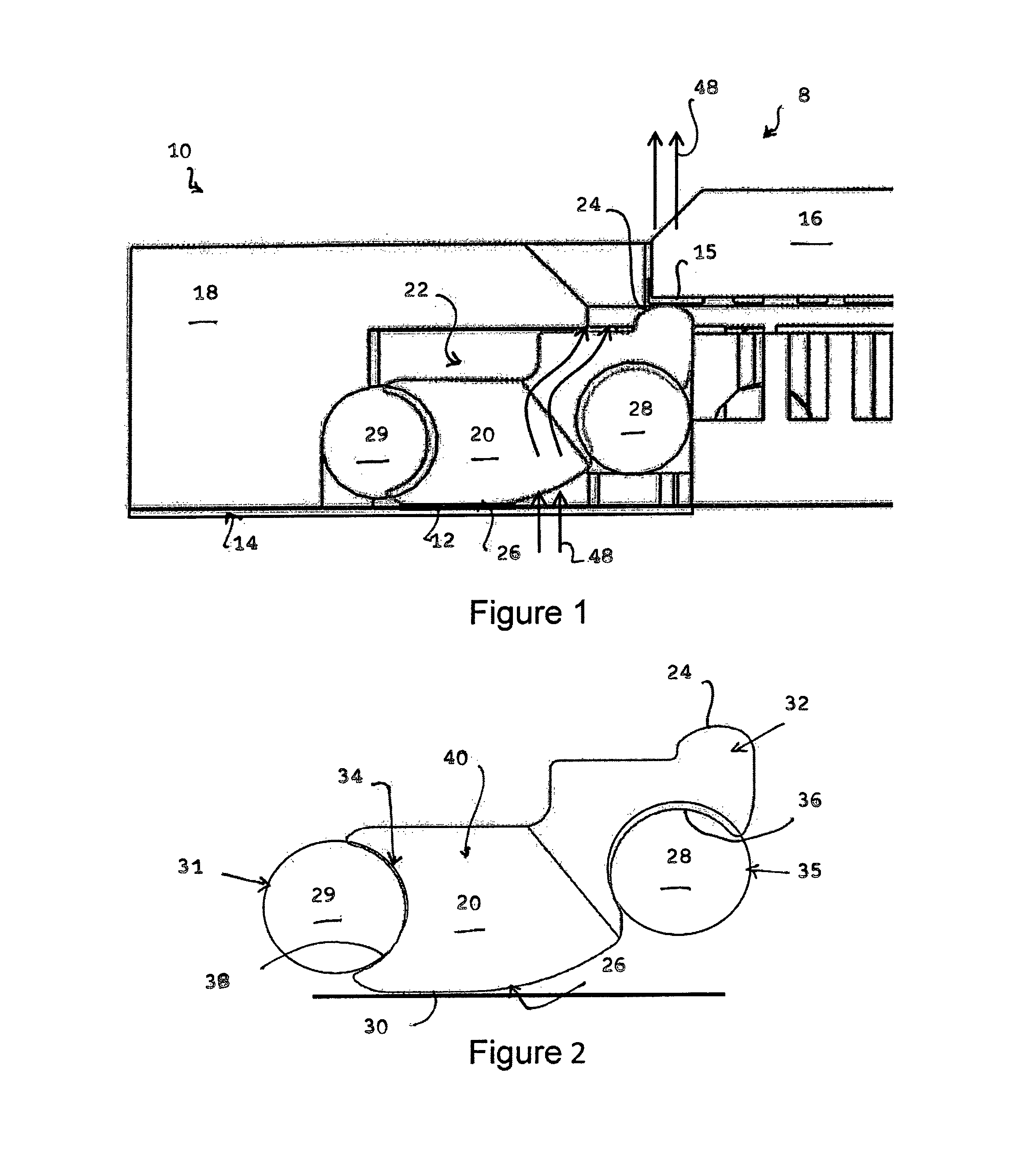
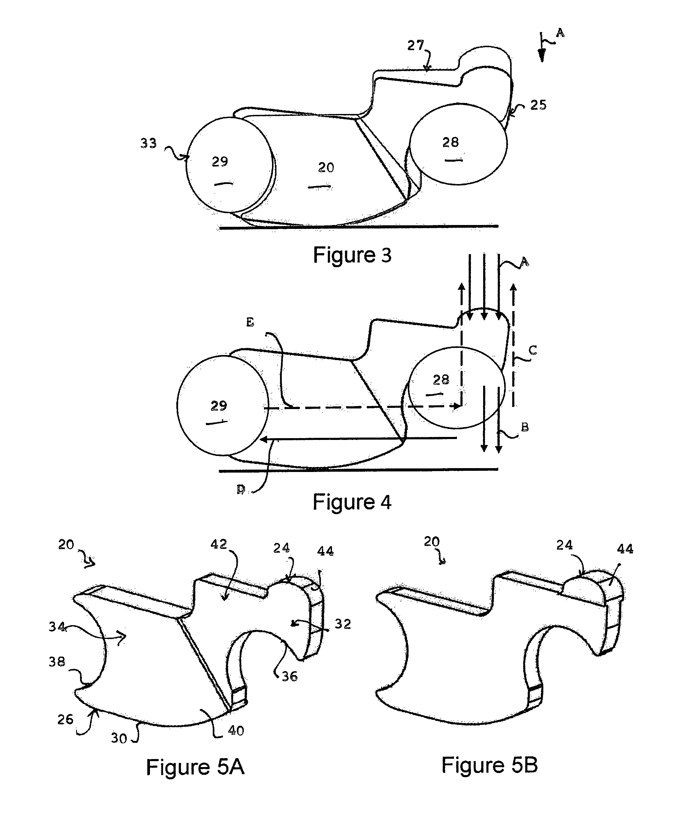
[0042]The interconnect assembly 10 comprises a housing 18 having a plurality of test contacts 20, as shown in FIG. 4, movably disposed in respective contact sockets 22 formed in the housing 18. Each of the test contacts 20 in this example is formed of elec...


PUM


Abstract

An electrical test contact electrically connects a test terminal of an Integrated Circuit (IC) test assembly with an IC terminal of an IC device in an electrical interconnect assembly. The test contact is formed of electrically conductive material and includes a head portion and a foot portion. The head portion includes a first electrical contacting portion for electrically engaging an IC terminal of an IC device during use, and the foot portion includes a second electrical contacting portion for electrically engaging a test terminal of a test assembly during use. The head portion includes a head receiving portion that receives a first resiliently biasing member to retain the first resiliently biasing member in contact with the test contact. The first resiliently biasing member biases the first electrical contacting portion against the IC terminal of the IC device during use. An electrical interconnect assembly having multiple test contacts is also disclosed.

Description

FIELD OF THE INVENTION[0001]The present invention relates to an electrical interconnect assembly for use in testing integrated circuit (IC) devices and to a test contact for use in an electrical interconnect assembly.BACKGROUND OF THE INVENTION[0002]As part of an IC manufacturing process, it is important to test manufactured IC devices in order to ensure that the devices are operating correctly and to required specifications. Such testing is generally carried out using an IC test system, the test system having a test assembly and an interconnect assembly arranged to electrically connect the test assembly with pads / leads of an IC during testing so that characteristics of the IC device in response to input electrical stimuli can be determined and compared with reference responses by the test assembly. The interconnect assembly comprises a series of test contacts which extend between respective test terminals of the test assembly and IC terminals of the IC device. The test assembly is ...

Claims


Application Information

Patent Timeline
Patent Type & Authority Patents(United States)
IPC IPC(8): G01R31/00H01R13/24G01R1/04
CPCH01R13/24G01R1/0466G01R1/0483H01R13/2407
Inventor FOONG, WEI KUONGGOH, KOK SINGMUNDIYATH, SHAMALLEE, ENG KIAT
Owner JF MICROTECH
Why Eureka
Try Eureka