Mask and method of forming pattern by using the same

a mask and pattern technology, applied in the field of masks and forming patterns, can solve the problems of affecting the resolution of the mask pattern transferred onto the photoresist layer, the width is subject to optical limitations, and the diffraction and interference of the mask pattern, so as to prevent the loading effect and correct the formation pattern corresponding

Active Publication Date: 2015-02-24
UNITED MICROELECTRONICS CORP
View PDF26 Cites 1 Cited by
  • Summary
  • Abstract
  • Description
  • Claims
  • Application Information

AI Technical Summary

Benefits of technology

[0007]An objective of the present invention is therefore to provide a mask including an assist pattern and a method of forming a pattern by using the same in order to increase the correctness of the formed pattern.
[0010]The present invention provides a mask including the assist pattern having at least an opening and a method of forming a pattern by using the same mask. In order to prevent the loading effect, the assist pattern is disposed in the second strip pattern neighboring the first strip pattern, and the width of the second strip pattern is substantially larger than the width of the first strip pattern. The assist pattern could be used to make uniform quantity of light passing through two sides of the first strip pattern in the lithography process, accordingly, the correctness of the formed pattern corresponding to the first strip pattern neighboring the second strip pattern can be improved.

Problems solved by technology

However, due to the optical proximity effect (OPE), the width is subject to optical limitations.
However, if the pitch is scaled down to a specific range, for example, equal to or smaller than half of the wavelength of light used in the exposure process, when the light passes through the mask, diffraction and interferences may occur, and the resolution of the mask pattern transferred onto the photoresist layer would be affected; in other words, due to the OPE, the deviation of the transferred pattern such as rounded right-angle corners, shortened line-ends, or increase / decrease of line widths would occur.
Furthermore, when light passes through the transparent regions of a mask having different interval sizes or different mask pattern densities, the light through the regions having small interval sizes is influenced by the transparent regions having large interval sizes, which may result in the deformation of the transferred pattern or a micro-loading effect.
Nevertheless, the dummy patterns will be transferred to photoresist layer, and the feasible utilization rate of the semiconductor wafer may decrease.
Moreover, the deposition of scattering bars reduces the feasible utilization rate of the mask and increases the layout budget of mask.
Consequently, when the mask includes the transparent regions having different interval sizes, a way to obtain the complete transferred patterns corresponding to the transparent regions having small interval size is still an important issue in the field.

Method used


Image

  • Mask and method of forming pattern by using the same
  • Mask and method of forming pattern by using the same
  • Mask and method of forming pattern by using the same

Examples


Embodiment Construction

[0018]To provide a better understanding of the present invention, preferred exemplary embodiments will be described in detail. The preferred exemplary embodiments of the present invention are illustrated in the accompanying drawings with numbered elements.

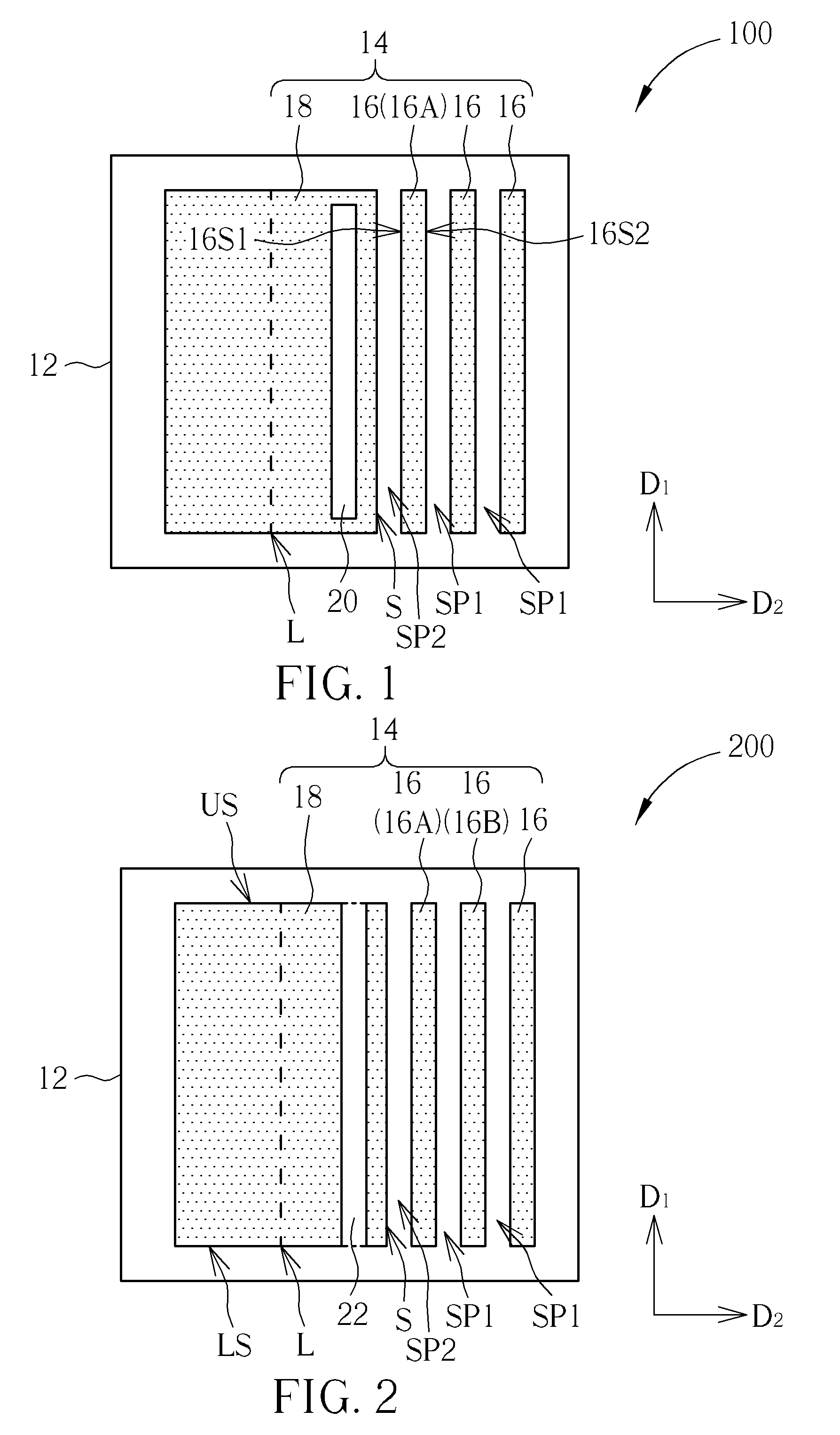
[0019]The present invention provides a mask. Please refer to FIG. 1, which is a schematic diagram illustrating a mask according to a first exemplary embodiment of the present invention. As shown in FIG. 1, the mask 100 includes a substrate 12, a plurality of strip patterns 14 and an assist pattern 20. The substrate 12 includes transparent substrate such as glass substrate, quartz substrate, plastic substrate or substrate made of proper transparent materials. The strip patterns 14 disposed on the substrate 12 are made of opaque material such as chromium (Cr). The strip patterns 14 include a plurality of printable features, and the printable features may include feature patterns used to construct integrated circuit (IC) such as doped...


PUM

PropertyMeasurementUnit
widthaaaaaaaaaa
widthaaaaaaaaaa
sizeaaaaaaaaaa

Abstract

A mask includes a substrate, at least a first strip pattern, at least a second strip pattern and an assist pattern. A width of the second strip pattern is substantially larger than a width of the first strip pattern. The assist pattern is disposed in the second strip pattern neighboring the first strip pattern, and the assist pattern does not overlap a center line of the second strip pattern.

Description

BACKGROUND OF THE INVENTION[0001]1. Field of the Invention[0002]The present invention relates to a mask and a method of forming a pattern, and more particularly, to a mask having an assist pattern and a method of forming a pattern by using the same mask.[0003]2. Description of the Prior Art[0004]With the trend of miniaturization of the electronic products and peripherals, research about thin structures and high integration of the semiconductor devices have become the essential subjects and developing aspects in the industry, and the lithography technology plays an important role to determine the performances of the semiconductor devices.[0005]In semiconductor manufacturing processes, the integrated circuit layout is first designed and formed as a mask pattern. The mask pattern is then proportionally transferred to a photoresist layer disposed on the semiconductor wafer through an exposure process followed by a development process. Subsequently, a corresponding etching process is per...

Claims


Application Information

Patent Timeline
Patent Type & Authority Patents(United States)
IPC IPC(8): G03F1/36
CPCG03F1/36G03F1/38G06F30/39
Inventor YANG, YU-SHIANG
Owner UNITED MICROELECTRONICS CORP
Why Eureka
Try Eureka