
Multi-layer amorphous silicon structure with improved poly-silicon quality after excimer laser anneal

a poly-silicon and amorphous technology, applied in the direction of coatings, metallic material coating processes, chemical vapor deposition coatings, etc., can solve the problem of limited grain size below 300 in current techniques, and achieve the effect of improving crystallinity and mobility of polycrystalline silicon

Active Publication Date: 2015-06-02
APPLIED MATERIALS INC
View PDF6 Cites 0 Cited by
  • Summary
  • Abstract
  • Description
  • Claims
  • Application Information

AI Technical Summary

Benefits of technology

The patent describes a way to improve the quality of polycrystalline silicon by using a multi-layer amorphous silicon structure. This helps to increase the crystallinity and mobility of the silicon.

Problems solved by technology

However, current techniques are limited to a grain size below 300˜500 nm.

Method used


Image

  • Multi-layer amorphous silicon structure with improved poly-silicon quality after excimer laser anneal
  • Multi-layer amorphous silicon structure with improved poly-silicon quality after excimer laser anneal
  • Multi-layer amorphous silicon structure with improved poly-silicon quality after excimer laser anneal

Examples


Embodiment Construction

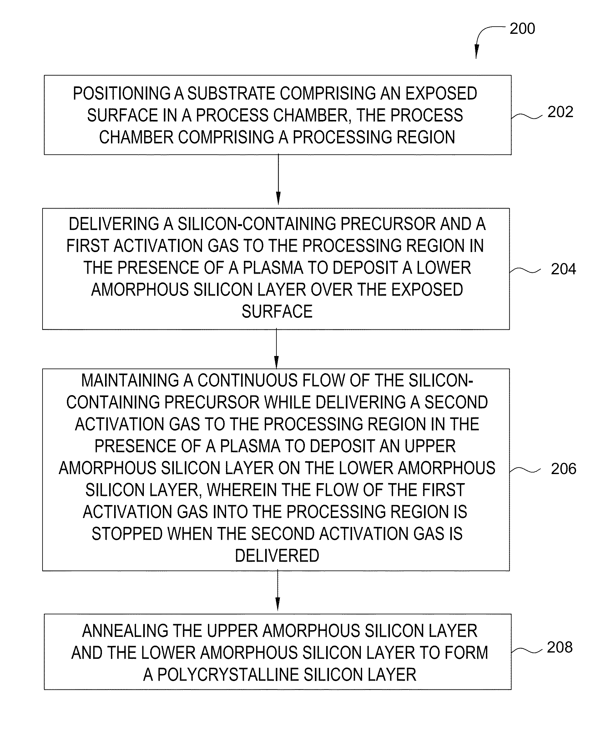
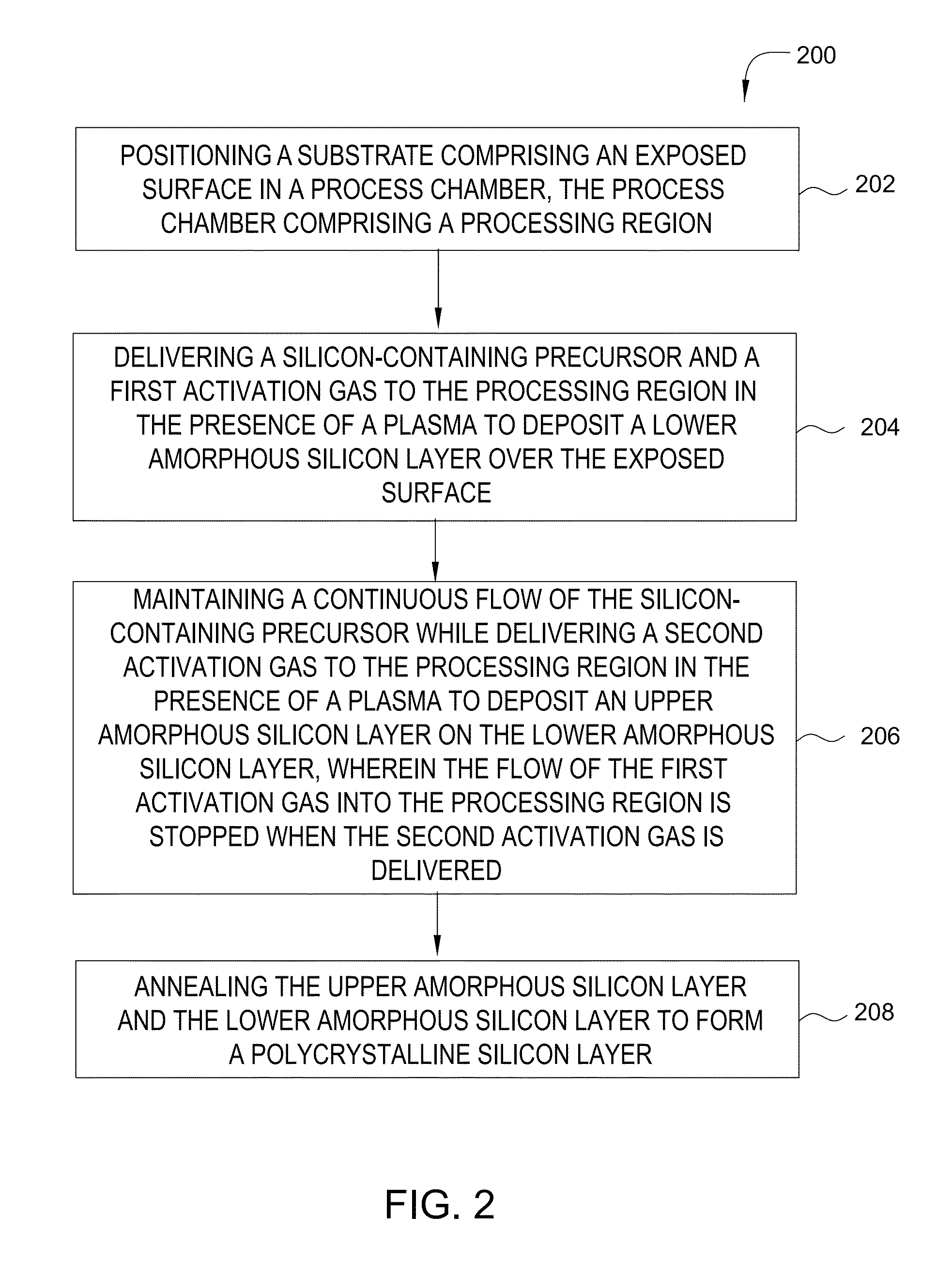
[0021]Embodiments disclosed herein generally relate to methods for forming a silicon-containing layer that may be used in TFT devices. The embodiments disclosed herein are more clearly described with reference to the figures below.

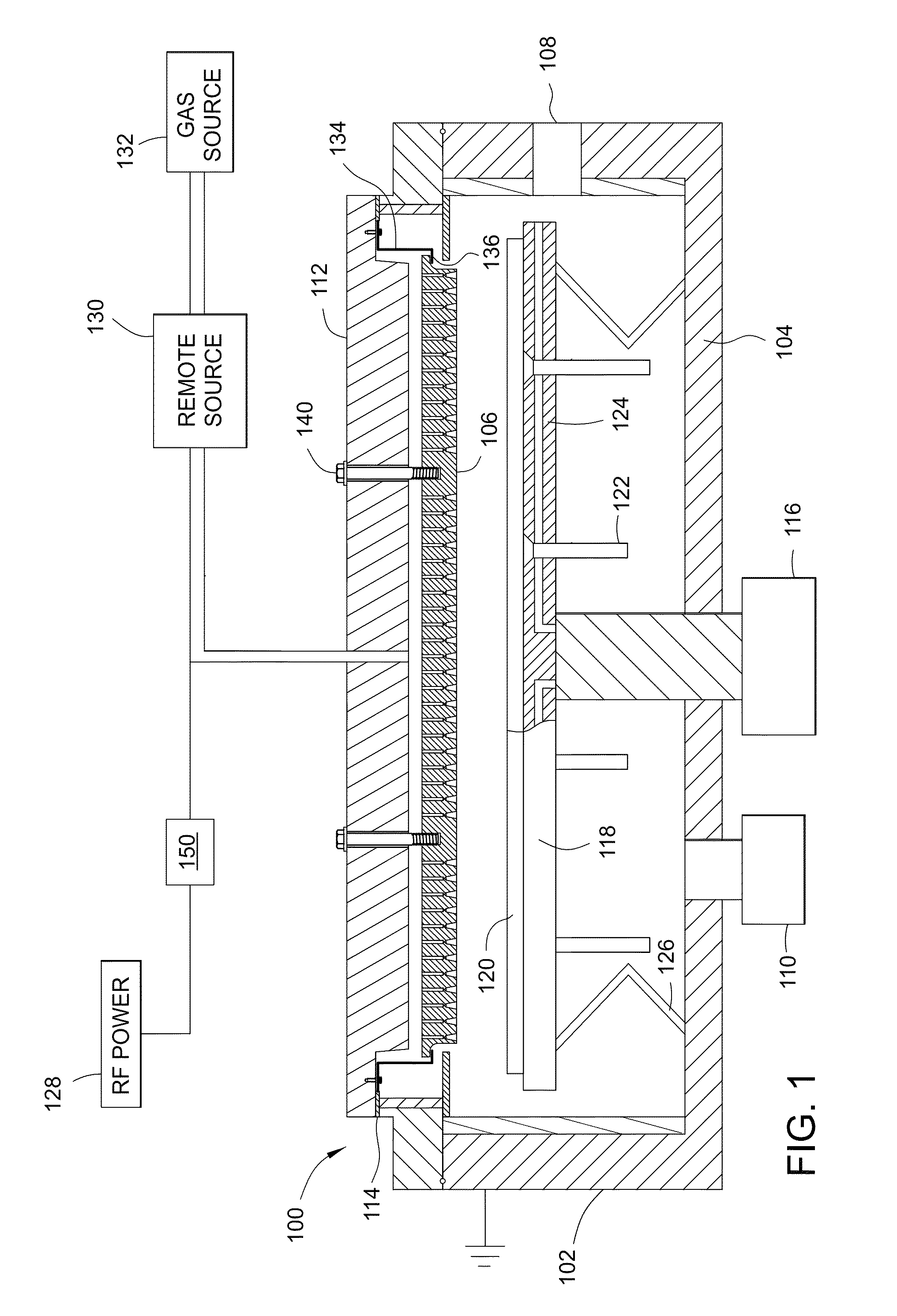
[0022]The invention is illustratively described below utilized in a processing system, such as a PECVD system available from AKT America, a division of Applied Materials, Inc., located in Santa Clara, Calif. However, it should be understood that the invention has utility in other system configurations, including those sold by other manufacturers.

[0023]FIG. 1 is a schematic, cross sectional view of an apparatus that may be used to perform the operations described herein. The apparatus includes a chamber 100 in which one or more films may be deposited onto a substrate 120. The chamber 100 generally includes walls 102, a bottom 104 and a showerhead 106 which define a process volume. A substrate support 118 is disposed within the process volume. The process vo...


PUM

PropertyMeasurementUnit
thicknessaaaaaaaaaa
temperatureaaaaaaaaaa
grain sizeaaaaaaaaaa

Abstract

The embodiments described herein generally relate to methods for forming a multi-layer amorphous silicon structure that may be used in thin film transistor devices. In one embodiment, a method includes positioning a substrate comprising a buffer layer in a process chamber, the process chamber comprising a processing region, forming a plurality of amorphous silicon layers and annealing the amorphous silicon layers to form a polycrystalline silicon layer. Forming the plurality of layers includes delivering a silicon-containing precursor and a first activation gas to the processing region to deposit a first amorphous silicon layer over the buffer layer, the silicon-containing precursor and the first activation gas being activated by a plasma and maintaining a continuous flow of the silicon-containing precursor while delivering a second activation gas, without the first activation gas, to the processing region to deposit a second silicon layer on the first silicon layer.

Description

CROSS-REFERENCE TO RELATED APPLICATIONS[0001]This application claims benefit of U.S. Provisional Patent Application Ser. No. 61 / 821,564, filed May 9, 2013, which is herein incorporated by reference.BACKGROUND[0002]1. Field[0003]Embodiments disclosed herein generally relate to methods for forming a silicon-containing layer. More particularly, embodiments herein relate to methods for forming a silicon-containing layer that may be used in thin film transistor (TFT) devices.[0004]2. Description of the Related Art[0005]Low Temperature Poly Silicon (LTPS) is commonly used as the channel layer in the next generation TFT display and Active Matrix Organic Light Emitting Diode (AMOLED) due to benefits including high mobility (>50 cm2 / Vs) and producibility under low temperature (<500° C.). LTPS is commonly produced using an amorphous silicon structure.[0006]A common method to crystallize the amorphous silicon structure in industry is through excimer laser annealing (ELA). Both film prope...

Claims


Application Information

Patent Timeline
Patent Type & Authority Patents(United States)
IPC IPC(8): H01L21/02
CPCH01L21/0262H01L21/02532H01L21/02592H01L21/02675H01L21/02488C23C16/24C23C16/4405C23C16/56
Inventor WANG, QUNHUAZHAO, LAICHOI, SOO YOUNG
Owner APPLIED MATERIALS INC
Learn More