Wireless IC tag and method for manufacturing wireless IC tag

a technology of ic tags and wireless coding, which is applied in the field of wireless ic tags, can solve the problems of inability to easily and inexpensively adjust the resonant frequency, and the conventional ic tag cannot be evaluated as sufficiently inexpensive, and achieves the effects of easy adjusting the length, simple structure and excellent communication characteristics

Inactive Publication Date: 2015-06-09
TATEYAMA KAGAKU KOGYO KK
View PDF33 Cites 0 Cited by
  • Summary
  • Abstract
  • Description
  • Claims
  • Application Information

AI Technical Summary

Benefits of technology

[0121]The present invention provides a less expensive IC tag that exhibits excellent communication characteristics, and a method for manufacturing thereof.
[0122]The present invention also provides an inexpensive IC tag having a simple structure that requires no additional component such as a capacitor, which allows easily adjusting the length of the antenna circuit as desired to thereby attain a predetermined resonant frequency, and a method for manufacturing such IC tag.

Problems solved by technology

Thus, the conventional IC tag cannot be evaluated as sufficiently inexpensive yet having excellent communication characteristics, and it is impossible to easily and inexpensively adjust the resonant frequency.Patented document 1: JP-A No. 2006-304184Patented document 2: JP-A No. 2001-010264Patented document 3: JP-A No. 2001-251115

Method used


Image

  • Wireless IC tag and method for manufacturing wireless IC tag
  • Wireless IC tag and method for manufacturing wireless IC tag
  • Wireless IC tag and method for manufacturing wireless IC tag

Examples


first embodiment

Structure of IC Tag

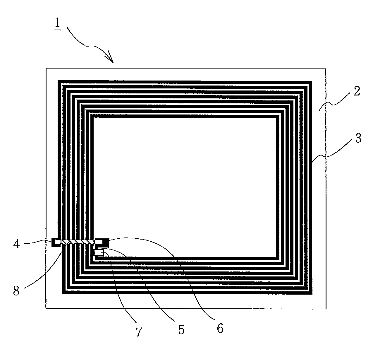
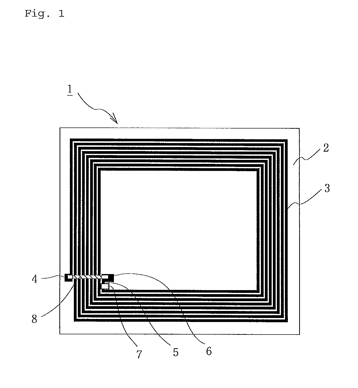
[0143]This embodiment will be described hereunder, based on the drawings. FIG. 1 is a schematic view showing an IC tag according to this embodiment.

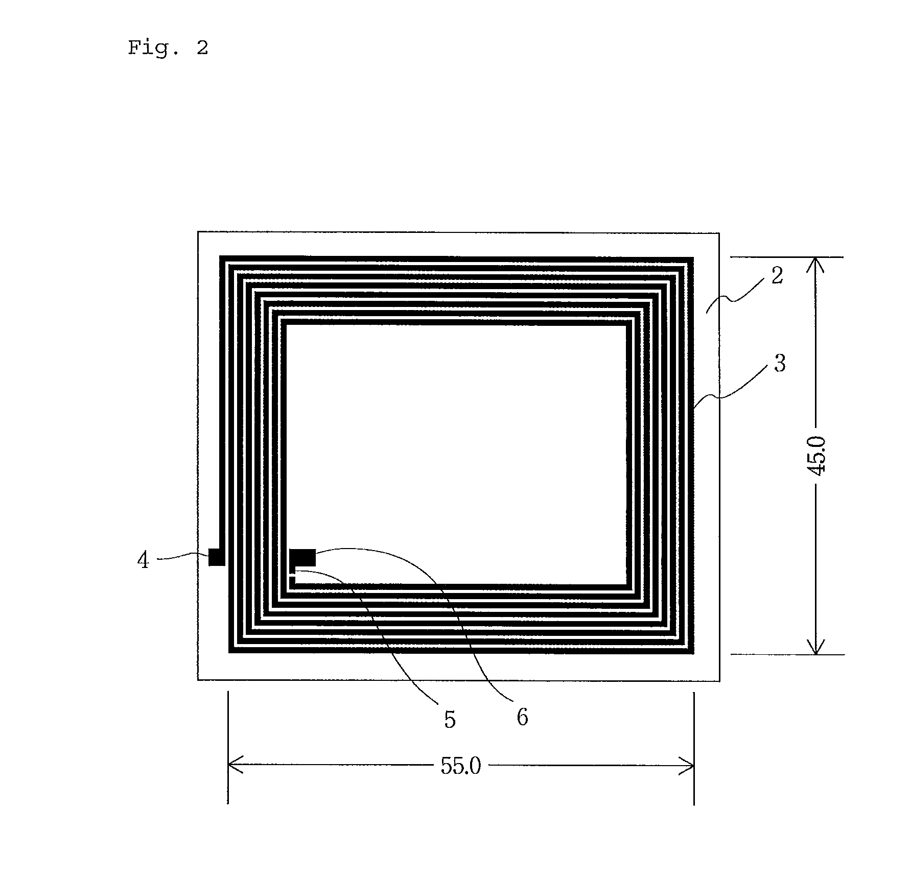
[0144]In FIG. 1, the reference numeral 1 designates an IC tag, and 2 a substrate (glassine paper manufactured by Lintec Corporation). Antenna circuits are denoted by 3 to 6, among which 4 and 6 designate the respective end portions of the antenna circuits. The numeral 7 designates an IC chip (I-CODE SLI manufactured by Philips Electronics N.V.), and two electrodes of the IC chip 7 (not shown) are each connected via the antenna circuit 3 and 5 respectively. The end portions 4 and 6 of the antenna circuit are connected via a jumper wire 8 (diameter 0.05 mm, coated with polyurethane in a thickness not less than 5 μm, manufactured by Riken Electric Wire Co., Ltd.).

[0145]The surface of the IC tag shown in FIG. 1 is finally laminated with a PET film (commercially available article, now shown) with a commercially available la...

second embodiment

Structure of IC Tag

[0166]According to the same procedures as in the first embodiment, except that a glassine paper (glassine W87.5 kg) was utilized as the substrate and one on the two patterns described in FIG. 4 was utilized as the pattern of the antenna circuit, the IC tag was made, and then subjected to a performance check.

[0167][Result of Performance Check]

[0168]The result of the performance check of the IC tag according to the second embodiment was as follows.[0169](i) impedance: 12 to 17Ω[0170](ii) resonant frequency (before laminating): 13.80 to 13.90 MHz[0171]resonant frequency (after laminating): 13.40 to 13.60 MHz[0172](iii) communication range (after laminating, aerial): 40 to 45 mm

third embodiment

[0173]According to the same procedures as in the first embodiment, except that a pattern described in FIG. 5 was utilized as the pattern of the antenna circuit, the IC tag was made, and then subjected to a performance check.

[0174][Result of Performance Check]

[0175]The result of the performance check of the IC tag according to the third embodiment was as follows.[0176](i) impedance: 14 to 16Ω[0177](ii) resonant frequency (before laminating): 14.50 to 14.60 MHz[0178]resonant frequency (after laminating): 14.10 to 14.30 MHz[0179](iii) communication range (after laminating, aerial): 35 to 40 mm

[0180]In view of the performance check result, it has been confirmed that in the IC tag according to the first to third embodiments, the antenna circuit was adequately formed, the IC chip and the antenna circuit were adequately connected, sufficiently small impedance was achieved, and a good characteristic was attained in communication range. It has also been confirmed that the IC chip was firmly ...


PUM

PropertyMeasurementUnit
temperatureaaaaaaaaaa
thicknessaaaaaaaaaa
thicknessaaaaaaaaaa

Abstract

A wireless IC tag which has an electrically insulative substrate, an antenna circuit provided on the surface of the substrate and an IC chip connected to the antenna circuit, wherein the antenna circuit is formed of solder and the IC chip is connected to the antenna circuit via the solder, andA wireless IC tag comprising an electrically insulative substrate, an antenna circuit provided on the surface of the substrate, an IC chip connected to the antenna circuit, and a jumper wire connected to the antenna circuit,wherein the antenna circuit is formed of a solder,the jumper wire is insulatively coated with a resin composition that evaporates, decomposes, or melts at a temperature not higher than a soldering temperature, andthe jumper wire is located on the same side of the substrate where the antenna circuit is provided.

Description

TECHNICAL FIELD[0001]The present invention relates to a wireless IC tag. More particularly, the present invention relates to a low-cost and thin wireless IC tag having an antenna circuit that offers excellent communication characteristics. The present invention also relates to an inexpensive wireless IC tag of a simple structure and modulated to a desired resonant frequency. Further, the present invention relates to a method for manufacturing the above-mentioned wireless IC tag.BACKGROUND ART[0002]The wireless IC tag (including a wireless IC card, and hereinafter generally referred to as “IC tag”) generally has an antenna circuit formed on a surface of an insulative substrate such as a resin film. An IC chip is mounted on the substrate carrying the antenna circuit, and connected to the antenna circuit.[0003]Because of carrying the IC chip, the storage capacity of the IC tag is far beyond that of a barcode or an ID tag, and also accepts free writing of additional information. In part...

Claims


Application Information

Patent Timeline
Patent Type & Authority Patents(United States)
IPC IPC(8): G06K19/06H01Q7/00H01Q1/22G06K19/077H05K3/22H05K1/16H05K3/34
CPCG06K19/07749G06K19/0775H01Q1/2225H01Q7/00H05K3/222Y10T29/49018H05K1/165H05K3/3421H05K3/3484H05K2201/10287H05K2201/10674H01L2224/16225H01L2224/32225H01L2224/73204H01L2224/83192H01L2924/00H05K3/3485
Inventor HONDA, KENICHI
Owner TATEYAMA KAGAKU KOGYO KK
Why Eureka
Try Eureka