Shrinkage of critical dimensions in a semiconductor device by selective growth of a mask material

a technology of selective growth and semiconductor devices, applied in semiconductor/solid-state device manufacturing, basic electric elements, electric devices, etc., can solve the problems of difficult to achieve the desired reduced lateral dimensions, affecting the finally achieved vertical and lateral etch rate, and requiring complex techniques for obtaining masks. achieve the effect of reducing the width of the previously formed mask opening, enhancing patterning strategies, and highly controllable manner

Inactive Publication Date: 2015-06-30
GLOBALFOUNDRIES INC
View PDF9 Cites 0 Cited by
  • Summary
  • Abstract
  • Description
  • Claims
  • Application Information

AI Technical Summary

Benefits of technology

[0014]Generally, the present disclosure contemplates manufacturing techniques in which the efficiency of patterning strategies may be enhanced by appropriately adjusting the width of mask openings on the basis of a selective material deposition so that, at least within a mask opening, additional material may be added in a highly controllable manner, thereby reducing the width of a previously formed mask opening. To this end, a plurality of selective deposition processes or strategies may be applied, such as wet chemical deposition techniques, plasma assisted techniques, thermally activated vapor deposition techniques and the like, so that the etch mask itself may be appropriately adapted in lateral size on the basis of a highly controllable deposition process, thereby avoiding sophisticated deposition and etch processes after completing the actual patterning process.
[0015]One illustrative method disclosed herein relates to forming an etch mask above a semiconductor device. The method comprises forming an opening in a mask layer that is formed above a material layer to be patterned, wherein the opening extends through the mask layer. The method further comprises performing a selective deposition process by initiating selective growth of material on an exposed surface of the mask layer so as to reduce a width of the opening.

Problems solved by technology

For example, currently in critical lithography steps, an exposure wavelength of 193 nm may be used, which, therefore, may require complex techniques for finally obtaining mask features having dimensions well below the exposure wavelength.
It turns out, however, that generally the width 133A may not substantially correspond to the desired target width of the openings 121A, thereby finally generating these openings with an increased width, which in turn may result in device failures or which may require an adapted device design in order to take into consideration the corresponding resolution capability of the patterning process for forming the openings 121A.
It is well known, however, that plasma assisted anisotropic etch recipes rely on process parameters, such as plasma power, reactive components in the plasma atmosphere, polymer residues and the like, which may affect the finally achieved vertical and lateral etch rate.
For example, silicon dioxide, which is a well-established dielectric material for passivating critical circuit elements, such as the gate electrode structures 110, may allow only a very moderate degree of tapering during the plasma assisted etch process so that it is very difficult to achieve the desired reduced lateral dimensions.
However, as indicated by the dashed lines, the actual contact elements 125A, 125B may have significantly greater lateral dimensions, thereby possibly contributing to increased yield loss, for instance by forming leakage paths or short circuits in critical areas 114.
Moreover, frequently, corresponding deposition processes and the subsequent patterning may be less than desirable in view of the finally obtained material characteristics, for instance if the patterning of sensitive low-k dielectric materials in metallization layers is considered.

Method used


Image

  • Shrinkage of critical dimensions in a semiconductor device by selective growth of a mask material
  • Shrinkage of critical dimensions in a semiconductor device by selective growth of a mask material
  • Shrinkage of critical dimensions in a semiconductor device by selective growth of a mask material

Examples


Embodiment Construction

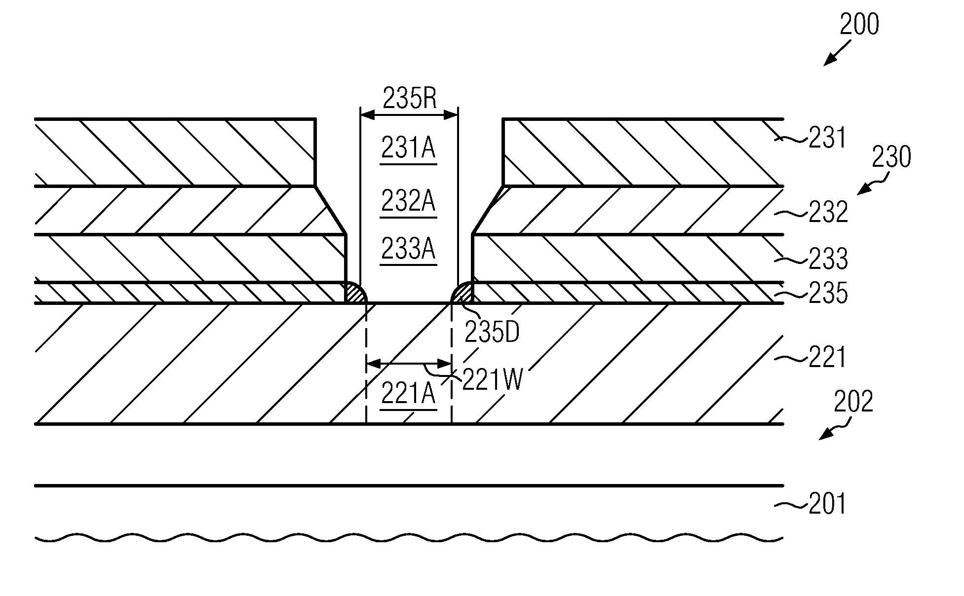
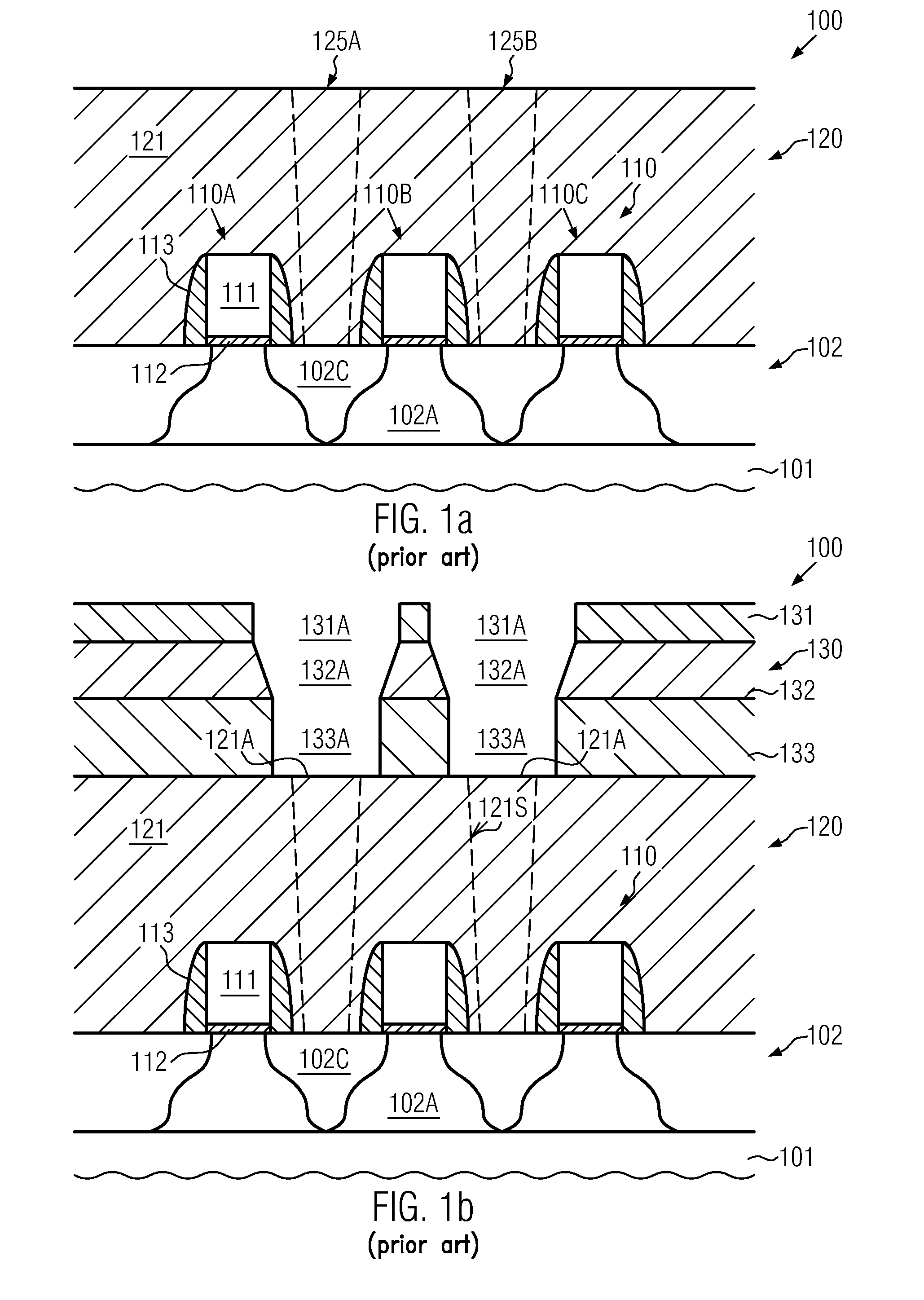
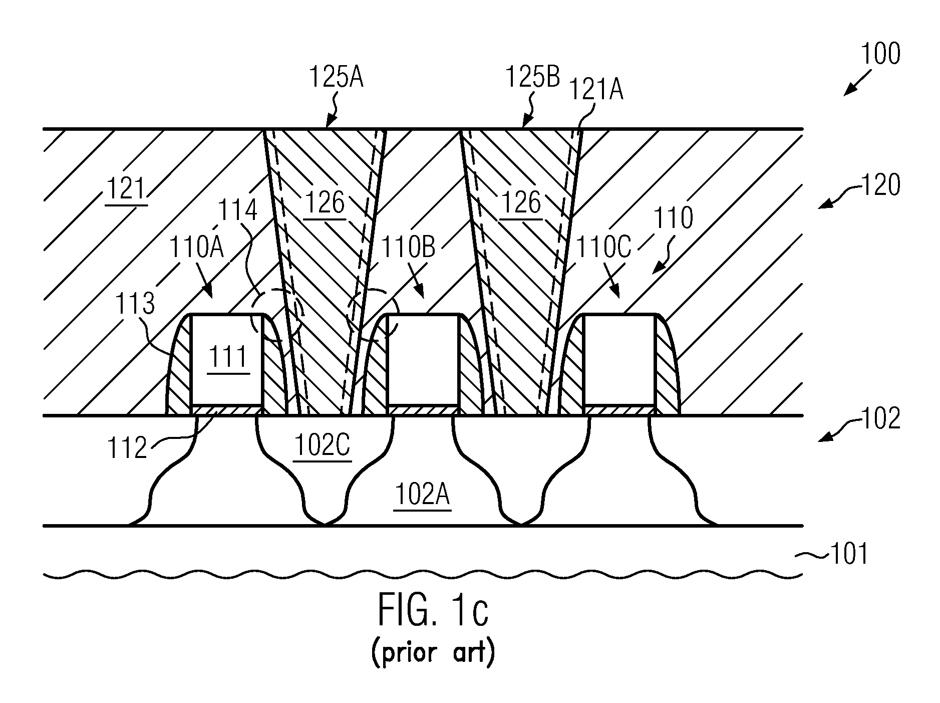
[0027]Various illustrative embodiments of the invention are described below. In the interest of clarity, not all features of an actual implementation are described in this specification. It will of course be appreciated that in the development of any such actual embodiment, numerous implementation-specific decisions must be made to achieve the developers' specific goals, such as compliance with system-related and business-related constraints, which will vary from one implementation to another. Moreover, it will be appreciated that such a development effort might be complex and time-consuming, but would nevertheless be a routine undertaking for those of ordinary skill in the art having the benefit of this disclosure.

[0028]The present subject matter will now be described with reference to the attached figures. Various structures, systems and devices are schematically depicted in the drawings for purposes of explanation only and so as to not obscure the present disclosure with details ...


PUM


Abstract

In sophisticated semiconductor devices, manufacturing techniques and etch masks may be formed on the basis of a mask layer stack which comprises an additional mask layer, which may receive an opening on the basis of lithography techniques. Thereafter, the width of the mask opening may be reduced by applying a selective deposition or growth process, which thus results in a highly uniform and well-controllable adjustment of the target width of the etch mask prior to performing the actual patterning process, for instance for forming sophisticated contact openings, via openings and the like.

Description

BACKGROUND OF THE INVENTION[0001]1. Field of the Invention[0002]The present disclosure generally relates to the field of semiconductor manufacturing, and, more particularly, to patterning techniques for forming device features having critical dimensions less than the resolution of optical lithography techniques.[0003]2. Description of the Related Art[0004]Semiconductor devices, such as advanced integrated circuits, typically contain a very large number of circuit elements, such as transistors, capacitors, resistors and the like, which are usually formed in a substantially planar configuration above an appropriate substrate having formed thereon a semiconductor layer. The fabrication of semiconductor devices, such as integrated circuits, requires tiny regions of precisely controlled size to be formed in one or more material layers provided above the substrate, such as a silicon substrate, a silicon-on-insulator (SOI) substrate, or other suitable carrier materials. These tiny regions ...

Claims


Application Information

Patent Timeline
Patent Type & Authority Patents(United States)
IPC IPC(8): H01L21/311H01L21/033H01L21/768
CPCH01L21/31144H01L21/0337H01L21/0338H01L21/76816
Inventor CHUMAKOV, DMYTROGRIMM, VOLKER
Owner GLOBALFOUNDRIES INC
Why Eureka
Try Eureka