Packaging of electronic circuitry

a technology of electronic circuitry and packaging, applied in the direction of semiconductor devices, semiconductor/solid-state device details, electrical apparatus, etc., can solve the problems of conventional fowl techniques that do not lend themselves or apply, and can suffer from a number of deficiencies

Active Publication Date: 2015-07-07
INFINEON TECH AMERICAS CORP
View PDF1 Cites 0 Cited by
  • Summary
  • Abstract
  • Description
  • Claims
  • Application Information

AI Technical Summary

Benefits of technology

[0017]In accordance with yet further alternative embodiments, the assembler can be configured to apply conductive adhesive above the layer of conductive material forming the drain node. To the adhesive, the assembler affixes a metal plate such as a heat sink. Via the heat sink above the layer of conductive material, heat generated by the circuit device can be safely dissipated.

Problems solved by technology

Conventional applications such as those as discussed above can suffer from a number of deficiencies.
In other words, conventional FOWL techniques do not lend themselves or apply when creating a fan-out wafer-level package for a two-sided circuit device (e.g., a chip having nodes on both facings).

Method used


Image

  • Packaging of electronic circuitry
  • Packaging of electronic circuitry
  • Packaging of electronic circuitry

Examples


Embodiment Construction

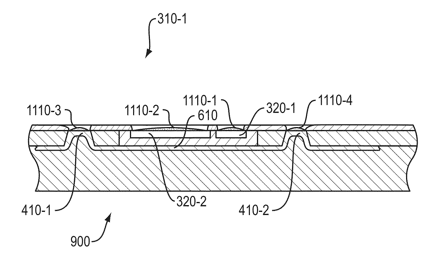
[0048]Embodiments herein are useful over conventional technology. For example, certain fan-out wafer level techniques as discussed herein support:

[0049]1.) producing electronic circuit packages of reduced size as a package can be just slightly larger than volume occupied by the outer dimensions of a circuit device such as a chip;

[0050]2.) producing electronic circuit packages at lower costs since many of the process steps can be done at a waferlevel, and most of the mechanical components are not discrete parts, but created in-situ on waferlevel;

[0051]3.) producing a switch device in an electronic circuit package to have lower RDSON values since the electrical pathway is minimized due to the small packages size;

[0052]4.) improving heat dissipation in an electronic circuit package since a heat dissipating elements can be integrated into the electronic circuit package;

[0053]5.) performing SFM metallization at a later processing stage, reducing a cost of fabricating an electronic circui...


PUM


Abstract

The present disclosure includes novel techniques to provide wafer level fan-outs in electronic circuit packages housing one or more circuit devices, at least one of which has input and / or output nodes disposed on opposite facings.

Description

RELATED APPLICATIONS[0001]This application is related to and claims the benefit of earlier filed U.S. Provisional Patent Application Ser. No. 61 / 604,966 entitled “FANOUT WAFERLEVEL PACKAGING FOR POWERCHIPS,” filed on Feb. 29, 2012, the entire teachings of which are incorporated herein by this reference.BACKGROUND[0002]Conventional Surface-Mount Technology (SMT) provides a way of interconnecting electronic circuit components. For example, according to conventional surface mount technology, electronic devices can be specifically packaged for subsequent mounting directly on a respective surface of a printed circuit board. Because of the advantages associated with surface mount technology such as smaller part size, surface mount technology has, to a large extent, replaced so-called through-hole technology in which wire leads of components are fitted and soldered into holes of a printed circuit board to alternatively provide connectivity.[0003]Surface mount devices can be packaged accord...

Claims


Application Information

Patent Timeline
Patent Type & Authority Patents(United States)
IPC IPC(8): H01L23/50H01L23/495
CPCH01L23/49541H01L2924/1306H01L23/367H01L21/561H01L21/568H01L23/5389H01L24/06H01L24/11H01L24/13H01L24/14H01L24/24H01L21/6835H01L24/73H01L24/82H01L24/92H01L24/96H01L2224/0401H01L2224/0603H01L2224/06181H01L2224/12105H01L2224/13014H01L2224/1403H01L2224/14051H01L2224/24137H01L2224/24195H01L2224/73259H01L2224/9222H01L2224/96H01L2924/10253H01L2924/1203H01L2221/68327H01L2221/68372H01L2924/181H01L2224/82H01L2224/11H01L2924/00012H01L2924/00
Inventor BIECK, FLORIANMONTGOMERY, ROBERT J.
Owner INFINEON TECH AMERICAS CORP
Why Eureka
Try Eureka