Wiring board and display apparatus

a display device and wiring board technology, applied in pulse generators, pulse techniques, instruments, etc., can solve the problems of likely short circuit between connection lines, and achieve the effect of reducing resistance differences

Active Publication Date: 2015-07-07
SHARP KK
View PDF11 Cites 8 Cited by
  • Summary
  • Abstract
  • Description
  • Claims
  • Application Information

AI Technical Summary

Benefits of technology

[0044]The wiring board of the present invention can reduce resistance difference between the lines of the multiple connection lines. In the display apparatus of the present invention, the frame region is narrow, short-circuit between the connection lines is less likely to occur, and deterioration in display quality such as occurrence of moire is less likely to occur.

Problems solved by technology

In the region where connection lines are disposed (frame region), each distance between adjacent connection lines tends to be made narrower as a result of frame downsizing, and thus electric short-circuit is likely to occur between the connection lines.

Method used


Image

  • Wiring board and display apparatus
  • Wiring board and display apparatus
  • Wiring board and display apparatus

Examples


embodiment 1

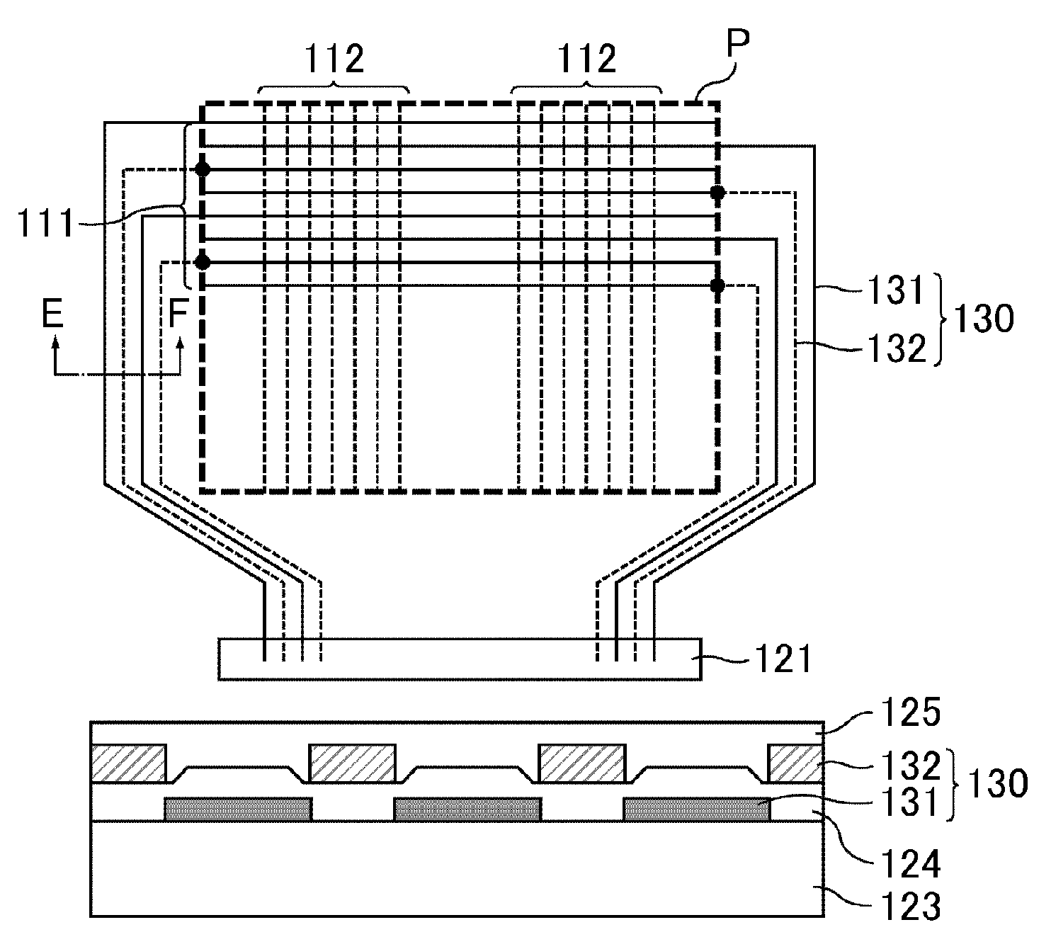
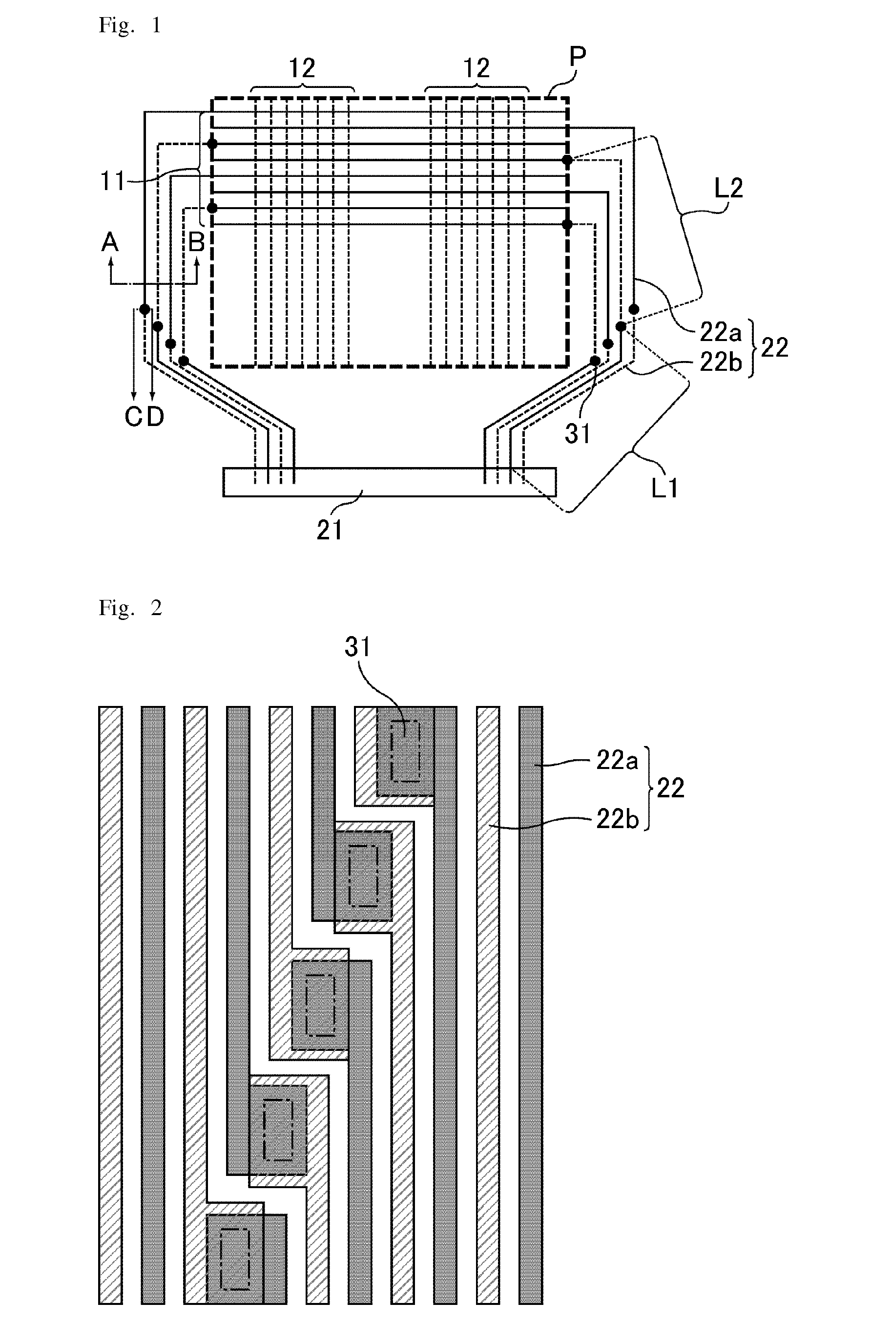
[0055]Embodiment 1 shows one example of the active matrix substrate (wiring board) of the present invention which can be used as a substrate of a liquid crystal display panel. FIG. 1 is a schematic plan view showing the line arrangement of the active matrix substrate of Embodiment 1. As shown in FIG. 1, the active matrix substrate of Embodiment 1 comprises a display region (control region) P provided with multiple gate lines 11 and multiple source lines 12. The gate lines 11 extend in the row direction and the source lines 12 extend in the column direction.

[0056]At positions adjacent to the respective intersections of the gate lines 11 and the source lines 12 are disposed TFTs which serve as switching elements, and each TFT is connected with a pixel electrode. The pixel electrode is an electrode disposed at a region (pixel) surrounded by gate lines 11 and source lines 12. When a gate voltage is applied to the TFTs through the gate lines 11, an image signal is supplied to the pixels ...

embodiment 2

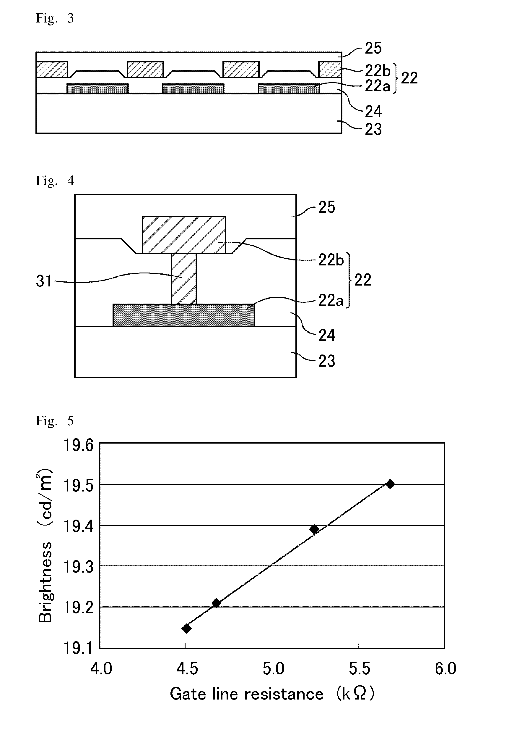
[0082]Embodiment 2 is one example of the active matrix substrate (wiring board) of the present invention which can be used as a substrate constituting a liquid crystal display panel. The active matrix substrate of Embodiment 2 is similar to the active matrix substrate of Embodiment 1 except that each source line comprises a gate metal portion and a source metal portion.

[0083]FIG. 6 is a schematic plan view showing the wiring structure of the active matrix substrate of Embodiment 2. As shown in FIG. 6, the active matrix substrate of Embodiment 2 comprises a display region (control region) P provided with multiple gate lines 11 and multiple source lines 12. The gate lines 11 extend in the row direction and the source lines 12 extend in the column direction. Multiple connection lines 42 formed from different materials extend from the source driver 41 in order alternately, and are connected with the corresponding source lines 12. The connection lines 42 extend in the column direction.

[0...


PUM

PropertyMeasurementUnit
lengthaaaaaaaaaa
polarityaaaaaaaaaa
weightaaaaaaaaaa

Abstract

The present invention provides a wiring board wherein the resistance difference between multiple connection lines is reduced. The wiring board of the present invention comprises: a control region and a peripheral region. The control region includes multiple gate lines extending in a row direction and multiple source lines extending in a column direction. The peripheral region includes a gate driver connected with the gate lines; a source driver connected with the source lines; and multiple connection lines which extend around the control region and which connect the gate driver with the gate lines. Each of the connection lines includes a gate metal portion formed from a material of the gate lines and a source metal portion formed from a material of the source lines. An insulating layer is disposed between the gate metal portion and the source metal portion. The gate metal portion and the source metal portion are connected with each other via a contact portion which penetrates the insulating layer.

Description

TECHNICAL FIELD[0001]The present invention relates to a wiring board and a display apparatus. The present invention specifically relates to a wiring board suitably used as a substrate constituting a panel of a display apparatus, and a display apparatus including the wiring board.BACKGROUND ART[0002]There is a demand for much smaller, lighter-weight portable electronic devices, such as mobile phones and PDA, equipped with a display panel such as a liquid crystal display panel or an organic electroluminescence display panel. In such situation, downsizing of vicinities of the display region, that is to say frame downsizing, tends to be intended and frame-downsizing techniques are eagerly developed.[0003]In these electronic devices, a display region is provided with multiple gate lines (scanning signal lines) and multiple source lines (image signal lines) so as to achieve high-definition display. The gate lines are driven by a gate driver and the source lines are driven by a source driv...

Claims


Application Information

Patent Timeline
Patent Type & Authority Patents(United States)
IPC IPC(8): G09G3/20H05K1/02G02F1/1345
CPCH05K1/0289G09G3/2092G02F1/13452H05K2201/10136
Inventor MORI, JUNICHI
Owner SHARP KK
Why Eureka
Try Eureka