Semiconductor device

a semiconductor and device technology, applied in the direction of semiconductor devices, transistors, electrical apparatus, etc., can solve the problems of significantly deteriorating the protection function of multi-finger transistors, more easily damaged integrated circuits, etc., and achieve the effect of decreasing the base resistance differen

Active Publication Date: 2017-02-07
UNITED MICROELECTRONICS CORP
View PDF11 Cites 3 Cited by
  • Summary
  • Abstract
  • Description
  • Claims
  • Application Information

AI Technical Summary

Benefits of technology

[0007]In view of the foregoing, this invention provides a semiconductor device, which is capable of decreasing the base resistance difference between central MOS element(s) and edge MOS element(s) as being applied as a multi-finger transistor.
[0012]In a case where the above semiconductor device serves as a multi-finger device for ESD, because the bottom depth of the electrical conduction path in the substrate in the first area closer to the pick-up region is smaller than that of the electrical conduction path in the substrate in the second area, a slight current bottleneck is present in the first area. As a result, the base resistance difference between the central MOS elements and the edge MOS elements of the multi-finger device is decreased, so the ESD current is not so concentrated in the central MOS elements as in the prior art, and the central MOS elements are prevented from damage.

Problems solved by technology

With continuous reduction in dimensions, the integrated circuits are more easily damaged by ESD, so ESD protection devices are usually designed in integrated circuits.
As a result, most ESD current will flow through the central NMOS, and contact spiking or junction punch easily occurs to the drain region thereof to significantly deteriorate the ESD protection function of the multi-finger transistor.

Method used


Image

  • Semiconductor device
  • Semiconductor device
  • Semiconductor device

Examples


Embodiment Construction

[0016]The following embodiments are intended to further explain this invention but not to limit the scope thereof. For example, though the semiconductor device described in the embodiments is a multi-finger MOS device for ESD, the semiconductor device of this invention may alternatively be a FinFET device. Moreover, although the first and second MOS elements are NMOS elements in the embodiments, they may alternatively be BJT elements, LDMOS (Laterally Diffused MOS) elements, or DDMOS (Double Diffused MOS) elements.

[0017]Further, though the first conductivity type is N-type and the second conductivity type is P-type in the embodiments, it is also possible that the first conductivity type is P-type and the second conductivity type is N-type.

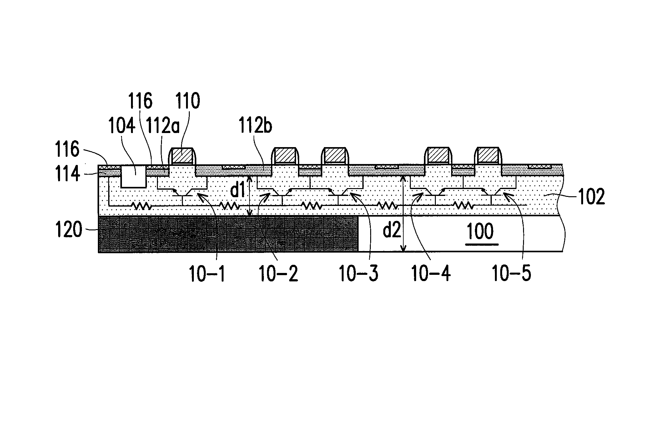
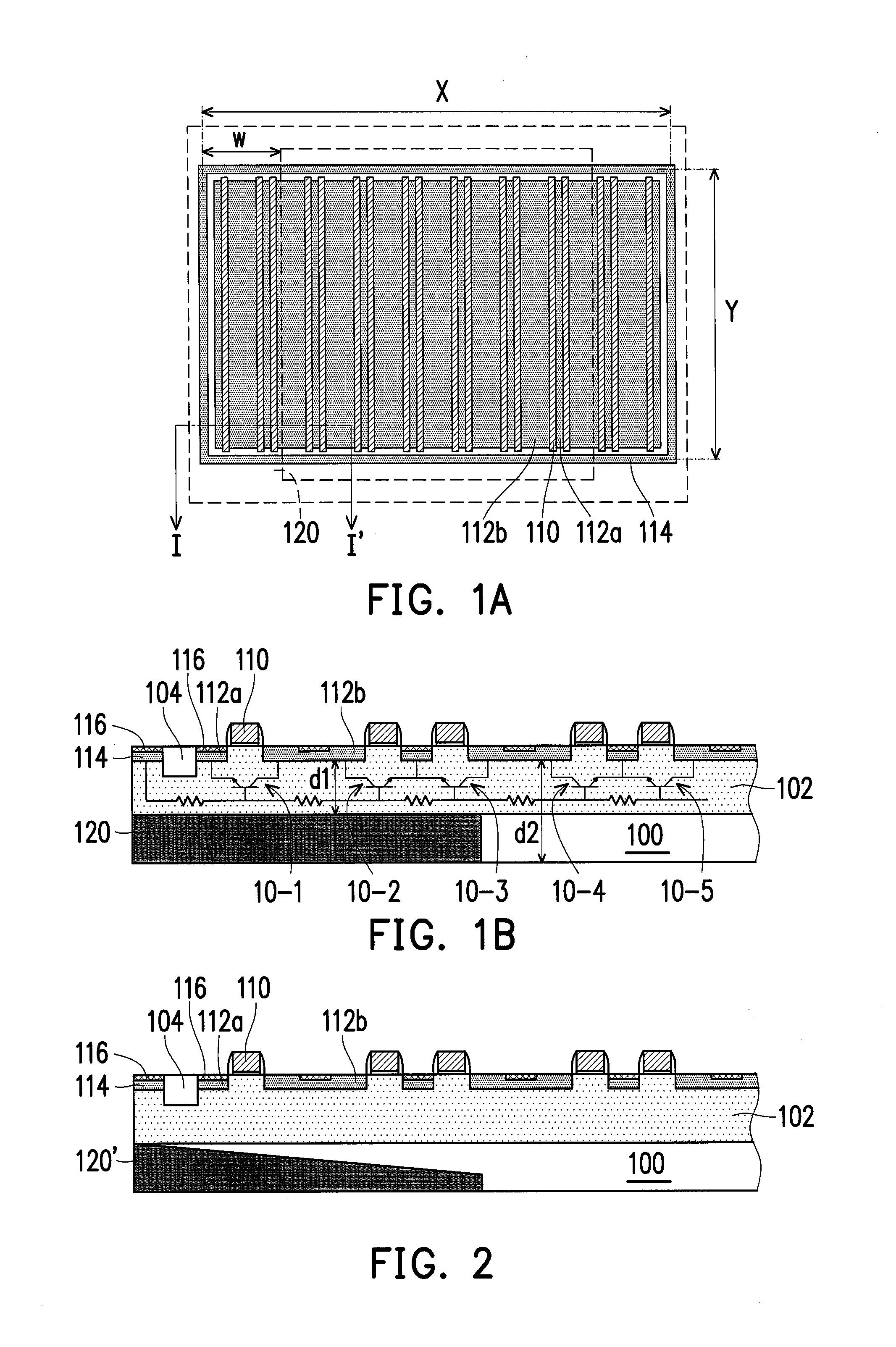
[0018]FIGS. 1A and 1B respectively illustrate a top view and an I-I′ cross-sectional view of a semiconductor device according to an embodiment of this invention.

[0019]Referring to FIGS. 1A and 1B, the semiconductor device includes a multi-finger MO...


PUM


Abstract

A semiconductor device is described, including a substrate including a first area and a second area, a first MOS element of a first conductivity type in the first area, and a second MOS element of the first conductivity type in the second area. The first area is closer to a pick-up region of the substrate than the second area. The substrate has a second conductivity type. The bottom depth of a first electrical conduction path in the substrate in the first area is smaller than that of a second electrical conduction path in the substrate in the second area.

Description

BACKGROUND OF THE INVENTION[0001]Field of Invention[0002]This invention relates to a structure of a semiconductor device, particularly a structure of an electrostatic discharge (ESD) device.[0003]Description of Related Art[0004]With continuous reduction in dimensions, the integrated circuits are more easily damaged by ESD, so ESD protection devices are usually designed in integrated circuits. One type of ESD protection device is the multi-finger transistor, which usually includes multiple NMOS elements arranged in parallel. The electrostatic discharge of such a device is based on the switching of the parasitic bipolar junction transistors (BJT) each formed by the source and drain regions of a NMOS element and the substrate.[0005]However, since the central NMOS elements are more distant from the pick-up regions of the substrate, the base resistance of the corresponding parasitic BJT is higher. Meanwhile, since the breakdown voltages of the drain regions of all NMOS elements are the s...

Claims


Application Information

Patent Timeline
Patent Type & Authority Patents(United States)
IPC IPC(8): H02H9/04H01L27/02H01L27/092H01L27/088
CPCH01L27/092H01L27/0277H01L27/088
Inventor WEN, YUNG-JUWANG, CHANG-TZUTANG, TIEN-HAOSU, KUAN-CHENG
Owner UNITED MICROELECTRONICS CORP
Why Eureka
Try Eureka