
Driving circuit and semiconductor device

a driving circuit and semiconductor technology, applied in the direction of pulse generators, electronic switching, pulse techniques, etc., can solve the problems of insufficient simple methods, difficult to reduce stray inductance, and heat dissipation capacity constraints, so as to reduce di/dt and achieve the effect of reducing the effect of other operations and minimal

Active Publication Date: 2015-07-28
MITSUBISHI ELECTRIC CORP
View PDF6 Cites 1 Cited by
  • Summary
  • Abstract
  • Description
  • Claims
  • Application Information

AI Technical Summary

Benefits of technology

[0013]It is an object of the present invention to provide a driving circuit capable of reducing di / dt in a turn-off switching operation of a MOSFET with minimum effect on the other operations.
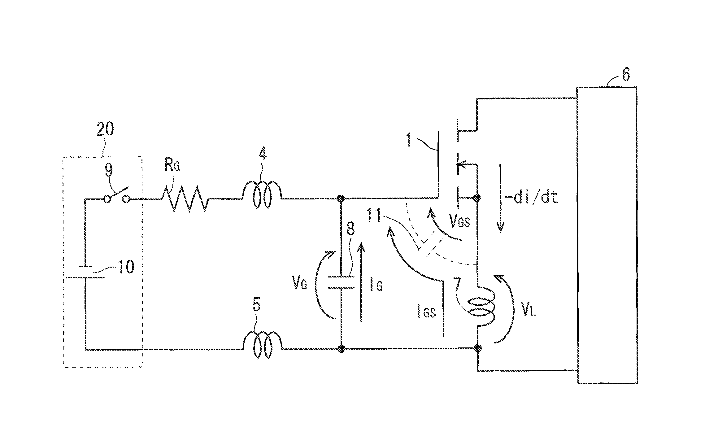
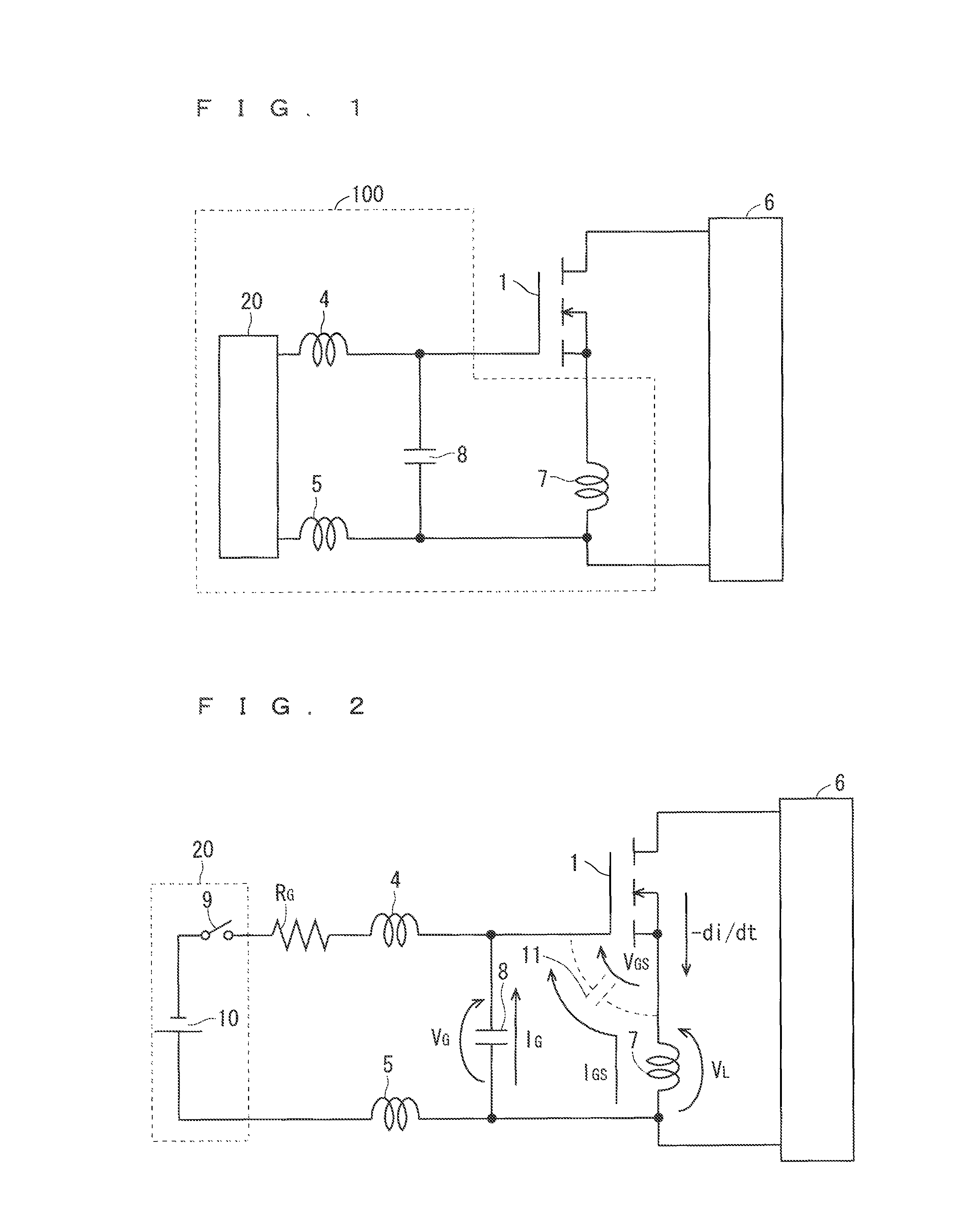
[0015]According to a driving circuit of the present invention, when turning off a switching element, a driving inductance is supplied with a current discharged by a capacitor, and thus a negative feedback voltage of a common inductor is effectively applied between a gate and a source of the switching element. Thus, when turning off the switching element, a change in time of the discharging current of an input capacitance of the switching element can be reduced. To reduce di / dt, increasing a gate resistance and decreasing the driving inductance are unnecessary, thereby having no effect on an operation except for turning off the switching element.

Problems solved by technology

In a case of employing the power MOSFET for a large current of 100 A or more, particularly 300 A or more, the current is large for turn-off speed of the MOSFET, so that di / dt as the ratio increases and it is difficult to reduce stray inductance (namely, self-inductance in which an interconnection obtains unintentionally) because the interconnection needs to be increased in a geometrical size to carry the large current.
However, the application of large current has a constraint on heat dissipation capacity of a heat loss by a switching loss, and in terms of saving energy, it is required to minimize the loss.
Thus, such simple method is not sufficient.
However, this timing changes under various conditions, and thus it is not easy to predict the timing from indirect parameters.
Under constraints of the present interconnection and heat dissipation technique, an inductance of an interconnection from the driving circuit to the MOSFET (hereinafter, referred to as “a driving inductance”) has a value which cannot be ignored for the inductance value appropriate for the negative feedback in the application of large current, and the driving inductance has a tendency to keep passing the driving current which interferes the negative feedback, thereby resulting in insufficient effects.

Method used


Image

  • Driving circuit and semiconductor device
  • Driving circuit and semiconductor device
  • Driving circuit and semiconductor device

Examples


first preferred embodiment

Configuration

[0030]FIG. 1 shows a configuration of a driving circuit 100 in the present preferred embodiment. The driving circuit 100 drives a switching element 1 connected to a main current circuit 6. In the present preferred embodiment, the switching element 1 is, for example, a MOSFET.

[0031]The driving circuit 100 includes a driving portion 20 applying voltage to a gate of the switching element 1 for turning on / off the switching element 1. The driving circuit 100 further includes a common inductor 7 and a capacitor 8. The common inductor 7 is disposed in an interconnection part commonly connected to the driving circuit 100 and a source side of the switching element 1 in a loop formed of the main current circuit 6 and the switching element 1. The capacitor 8 is connected between the gate side and the source side of the switching element 1 on the driving portion 20 side with respect to the common inductor 7.

[0032]Driving inductances 4 and 5 are self-inductances of an interconnectio...

second preferred embodiment

Configuration

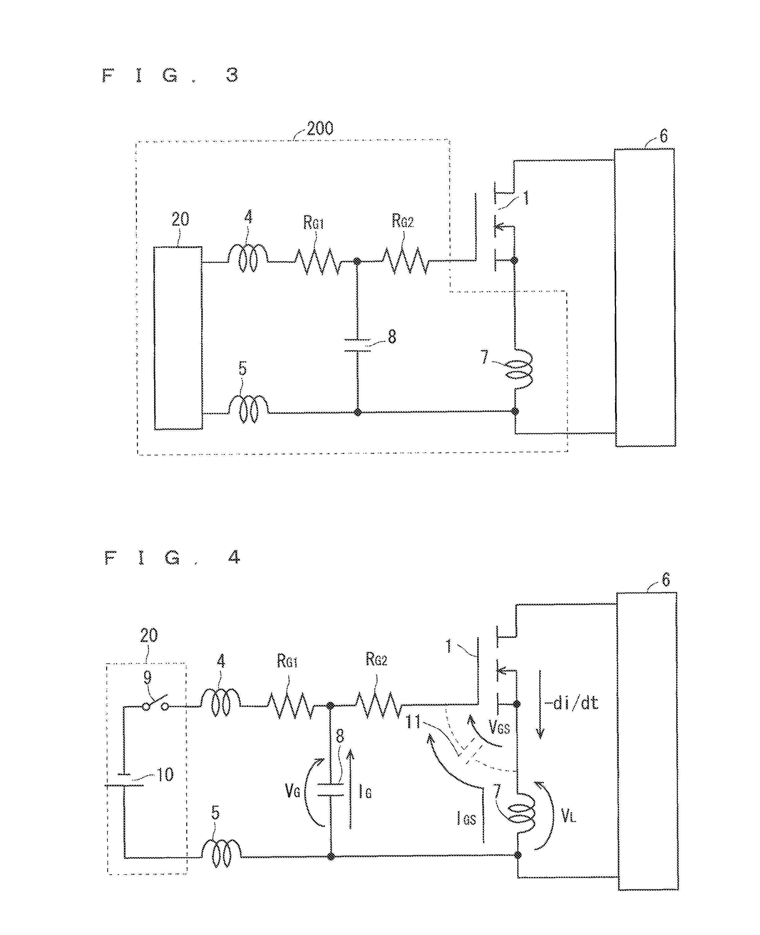
[0049]FIG. 3 shows a configuration of a driving circuit 200 in the present preferred embodiment. In the present preferred embodiment, a plurality of driving current limiting portions connected in series are provided on a gate side of a switching element 1. As shown in FIG. 2, the driving current limiting portions are, for example, gate resistances RG1 and RG2. An end of a capacitor 8 is connected between the gate resistances RG1 and RG2.

[0050]

[0051]A negative feedback voltage corresponding to driving inductances 4 and 5 is 1.6 V similarly to the first preferred embodiment. On the other hand, to make a discharging current of an input capacitance 11 one-fifth thereof, the voltage applied to the gate resistance RG2 is made one-fifth. The necessary negative feedback voltage corresponding to the gate resistance is 12 [V]×RG2 / (RG2+RG1)=12 [V]×1 / (1+RG1 / RG2), and the ratio of the gate resistance RG1 to the gate resistance RG2 can adjust the amount of the negative feedback. Sinc...

third preferred embodiment

Configuration

[0059]FIG. 6 shows a configuration of a driving circuit 300 in the present preferred embodiment. In the present preferred embodiment, two switching elements 1a and 1b (MOSFETs) are connected in parallel to a main current circuit 6.

[0060]Similar to the first preferred embodiment, common inductors 7a and 7b are provided on a source side of the switching elements 1a and 1b, respectively. A capacitor 8a is connected between the gate side and the source side of the switching element 1a on the side closer to a driving portion 20 than the common inductor 7a with respect to the switching element 1a. Similarly, a capacitor 8b is connected between the gate side and the source side of the switching element 1b on the side closer to the driving portion 20 than the common inductor 7b with respect to the switching element 1b. An interconnection has the driving inductances 4 and 5.

[0061]

[0062]In a case where the switching element 1a switches faster than the switching element 1b, the sw...


PUM


Abstract

A driving circuit of the present invention drives a switching element connected to a main current circuit. The driving circuit includes a driving potion applying on / off-voltage to a gate of the switching element, a common inductor disposed in an interconnection part commonly connected to the driving circuit and a source side of the switching element in a loop formed of the main current circuit and the switching element, and a capacitor connected between the gate side and the source side on the driving portion side with respect to the common inductor.

Description

BACKGROUND OF THE INVENTION[0001]1. Field of the Invention[0002]The present invention relates to a driving circuit and a semiconductor device, and more particularly, to a driving circuit that drives a switching element connected to a main current circuit of high voltage large current. For example, it relates to a driving circuit that drives a high-speed switching element, such as a MOSFET, and particularly, a switching element including a wide bandgap semiconductor. Moreover, it relates to a semiconductor device including the driving circuit.[0003]2. Description of the Background Art[0004]Conventionally, in a case where “a semiconductor switch group represented by a MOSFET” (hereinafter, simply referred to as a “MOSFET”) such as a power MOSFET (a hybrid switch of a MOSFET and a J-FET) is used for power equipment, it is mainly used as discrete components for a switching power supply and the like. To make full use of the MOSFET having high speed performances, a switching speed has bee...

Claims


Application Information

Patent Timeline
Patent Type & Authority Patents(United States)
IPC IPC(8): H03K3/00H03K17/16
CPCH03K17/165H03K17/167
Inventor TABATA, MITUHARUMIYAZAKI, YUJI
Owner MITSUBISHI ELECTRIC CORP
Learn More