On-chip bad block management for NAND flash memory
a technology of bad block management and nand flash memory, applied in the direction of memory adressing/allocation/relocation, instruments, input/output to record carriers, etc., can solve the problem of memory being susceptible to bad block conditions
- Summary
- Abstract
- Description
- Claims
- Application Information
AI Technical Summary
Problems solved by technology
Method used
Image


Examples
Embodiment Construction
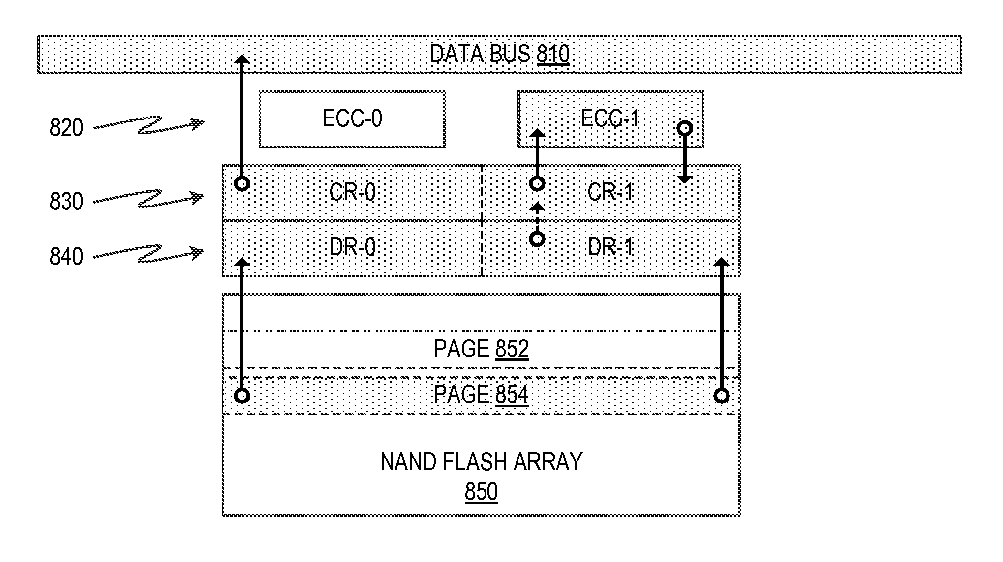
[0032]Using a host device or an outside controller to implement the bad block Look-Up Table (“LUT”) in software or hardware adds overhead in software development and possibly hardware cost. However, certain functions relating to creation and use of the LUT may be implemented “on chip” in the memory device itself, that is on the same die in an additional circuit, or even within the command and control logic of the memory device, so as to reduce the overhead. Moreover, the on-chip implementation of the LUT may be tightly integrated with other functions of the command and control logic to enable powerful new commands for NAND flash memory, such as a continuous read command and variations thereof.
[0033]FIG. 1 is a schematic functional block diagram of a NAND flash memory device 20 which includes a NAND flash array 40 and associated page buffer 38. The NAND flash array 40 includes word (row) lines and bit (column) lines, and is organized into a user-addressable area 42, a redundant block...
PUM
 Abstract
Description
Claims
Application Information