Touch panel having a shielding structure and method of manufacturing the same

a technology of shielding structure and touch panel, which is applied in the field of touch panel, can solve the problems of low shielding layer impedance, inability to avoid noise interference from electronic devices, and weak shielding noise effect, and achieve the effect of reducing noise interferen

Active Publication Date: 2015-09-15
TPK TOUCH SOLUTIONS (XIAMEN) INC
View PDF20 Cites 0 Cited by
  • Summary
  • Abstract
  • Description
  • Claims
  • Application Information

AI Technical Summary

Benefits of technology

[0008]In view of the above-mentioned, the present disclosure provides a touch panel having a shielding structure and a method of manufacturing the same, using a wrap-around conductive ring to electrically connect the shielding layer such that impedance of the shielding layer is consistent even if the distance between the shielding layer and the shielding pin is different, thereby solving the problem of noise interference.
[0011]By means of the touch panel with a shielding structure provided in the present disclosure, impedance of the shielding layer will be consistent for different distances between the shielding layer and the FPC, to eliminate noise interference from a liquid crystal display or an electronic device under the touch panel, while using the touch panel.

Problems solved by technology

However, impedance of the shielding layer is low at the FPC end and is high at the end far away from the FPC.
Also, effect of the shielding noise is weakened by inconsistency in impedance of the shielding layer.
Thus, noise interference from the electronic device cannot be avoided when using the touch panel.

Method used


Image

  • Touch panel having a shielding structure and method of manufacturing the same
  • Touch panel having a shielding structure and method of manufacturing the same
  • Touch panel having a shielding structure and method of manufacturing the same

Examples


Embodiment Construction

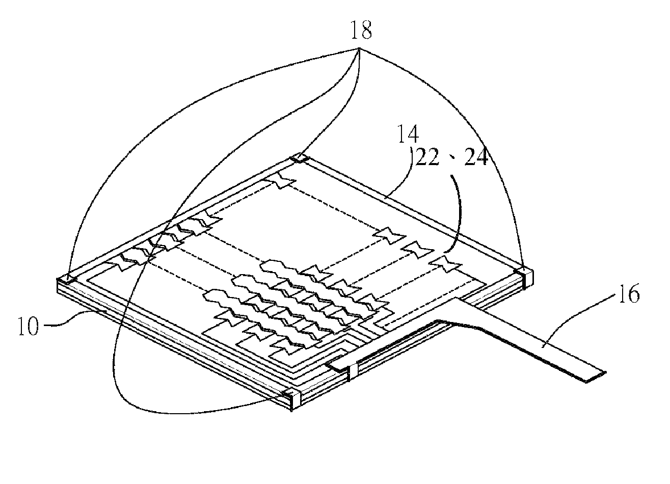
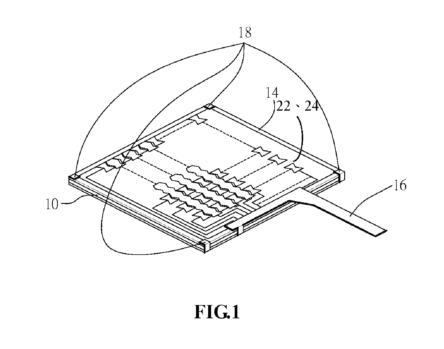
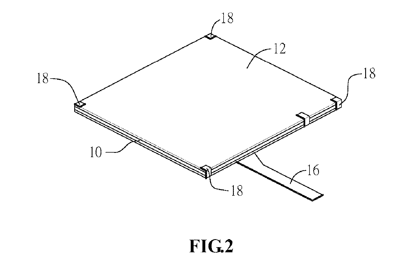
[0018]FIG. 1 and FIG. 2 show a touch panel having a shielding structure in accordance with the present disclosure. The touch panel having a shielding structure comprises a substrate 10, a shielding layer 12, a conductive ring 14 and a plurality of conductive connection points 18. The conductive ring 14 is disposed on periphery of an upper surface of the substrate 10 of the touch panel and the shielding layer 12 is disposed on a lower surface of the substrate 10. The shielding layer 12 is a conductive layer, such as a metal layer or an Indium tin Oxide (ITO) layer. The touch panel having a shielding structure further comprises a plurality of electrodes 22 and 24 surrounded by the conductive ring 14. In different embodiments, the conductive ring 14 can be made of a metal or a transparent conductive material, such as ITO or a combination thereof. The conductive ring 14 is electrically connected to a shielding pin of a FPC. In different embodiments, the shielding layer 12 is a plane str...


PUM

PropertyMeasurementUnit
shielding structureaaaaaaaaaa
conductiveaaaaaaaaaa
shieldingaaaaaaaaaa

Abstract

The present disclosure relates to a touch panel having a shielding structure and a method of manufacturing the same. The touch panel having a shielding structure comprises a conductive ring disposed on periphery of an upper surface of a substrate, a shielding layer disposed on a lower surface of the substrate, and a plurality of conductive connection points electrically connecting the shielding layer and the conductive ring. By connecting the shielding layer and the conductive ring by the conductive connection points, impedance of the shielding layer is consistent for different distances between the shielding layer and flexible printed circuit, thereby eliminating noise interference from a liquid crystal display or an electronic device under the touch panel, while using the touch panel. Moreover, the manufacturing method of the touch panel with a shielding structure is a simple process, which reduces the manufacturing cost.

Description

[0001]This application claims the benefit of Chinese application No. 201110281019.4, filed on Sep. 10, 2011.BACKGROUND OF THE INVENTION[0002]1. Field of the Invention[0003]The present disclosure relates to a touch panel, especially to a touch panel having a shielding structure and method of manufacturing the same.[0004]2. Description of the Related Art[0005]Touch panels can, based on different sensing principles, be classified into resistive type, capacitive type, acoustic wave type, optical type and so on. Touch panels typically determine a touch location by detecting changes in electrical signals, optical signals and acoustic wave signals.[0006]In a conventional electronic device integrated with a touch panel, a shielding layer is formed between the touch panel and the electronic device, and one end of the shielding layer is electrically connected to a shielding pin of a flexible printed circuit (FPC). The shielding layer can absorb noise from the electronic device, and the noise ...

Claims


Application Information

Patent Timeline
Patent Type & Authority Patents(United States)
IPC IPC(8): H01H1/10G06F3/041
CPCG06F3/041G06F2203/04103G06F2203/04107Y10T29/49155Y10T29/49162Y10T29/49165
Inventor YE, HUILINYU, JINGLIN, QUNFENG
Owner TPK TOUCH SOLUTIONS (XIAMEN) INC
Why Eureka
Try Eureka