High rate electric field driven nanoelement assembly on an insulated surface
a technology of electric field and nanoelement, which is applied in the direction of electrolysis, metallic pattern materials, electroforming by electrophoresis, etc., can solve the problems of limited assembly on conductive substrates, method is fast, and assembly typically takes less than a minu
- Summary
- Abstract
- Description
- Claims
- Application Information
AI Technical Summary
Benefits of technology
Problems solved by technology
Method used
Image
Examples
example 1
Nanoparticle Assembly
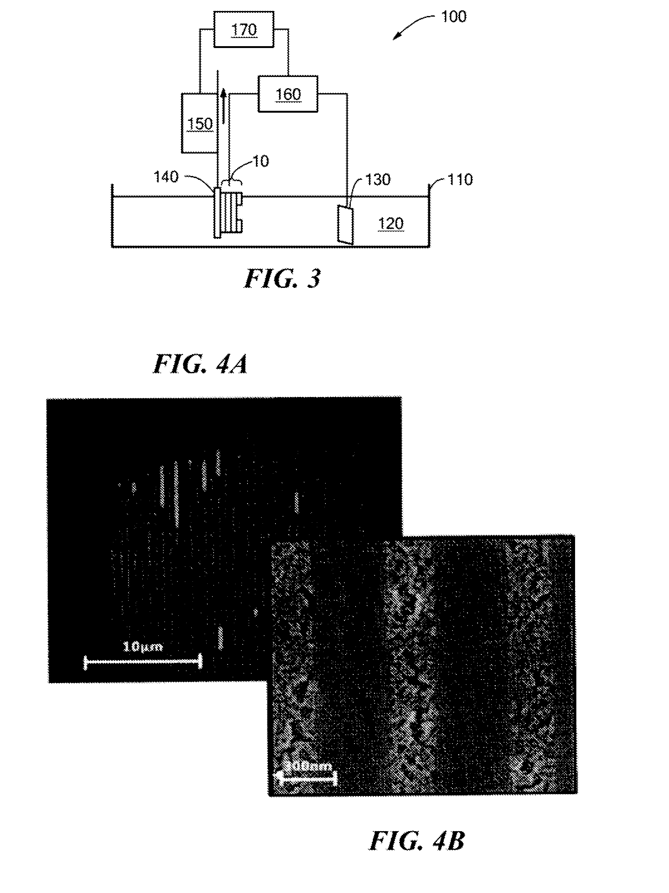
[0042]A patterned substrate was prepared having vertically oriented nanotrenches. The trenches were 300 nm wide, 50 μm long, and 150 nm deep. The substrate was submerged into a suspension having wt % of 48 nm polystyrene latex nanoparticles (Thermoscientific) at a pH of 10.9. The counter electrode was placed at 5 mm from the substrate, and a voltage of 3.4V (positive at the substrate, negative at the counter electrode) as the substrate was pulled through the suspension surface at 3 mm / min using a KSV NIMA Dip Coater Single Vessel System. The assembly result is presented in FIG. 4, showing low and high magnification SEM images. The assembly (dark areas) covered nearly the entire substrate. The high magnification inset shows that the assembled nanoparticles completely filled the trenches and that assembly was limited to the trenches.
example 2
Effect of Applied Voltage on Nanoparticle Assembly
[0043]Nanoparticle assembly was carried out under the conditions of Example 1, but using a pull rate of 5 mm / min and varying the applied voltage as shown in the SEM images of FIG. 5. There was no assembly at 0V and 2V. Assembly started at 2.3V, increasing with voltage. Nearly complete assembly was obtained at 2.7V, and assembly was essentially 100% complete at 3V.
example 3
Nanoparticle Assembly into Different Two Dimensional Void Patterns
[0044]Polystyrene latex nanoparticles (48 nm) were assembled in different void patterns, including nanotrenches (300 nm wide, 5 μm long, 150 nm deep) having vertical, horizontal, diagonal, and intersecting orientations, as shown in the SEM images of FIG. 6. The results confirmed that assembly can be completed with complete selectivity for the pattern voids in any two-dimensional pattern. For the experiments depicted in FIG. 6, the pull rate was 1-3 mm / min, the voltage was 2.9-3.1V, the nanoparticle concentration was 1 wt %, the pH was 10.9-11.1, and the counter electrode was 5 mm removed from the substrate.
PUM
| Property | Measurement | Unit |
|---|---|---|
| thickness | aaaaa | aaaaa |
| thickness | aaaaa | aaaaa |
| electrical potential | aaaaa | aaaaa |
Abstract
Description
Claims
Application Information


