Pattern synthesis apparatus and semiconductor test system having the same

a technology of semiconductor test system and synthesis apparatus, which is applied in the direction of electronic circuit testing, measurement devices, instruments, etc., can solve the problems of parametric failure, non-defective units may not operate properly when mounted in personal computers or user devices, and memory modules or devices which are commercially available after

Active Publication Date: 2016-01-05
SAMSUNG ELECTRONICS CO LTD
View PDF10 Cites 0 Cited by
  • Summary
  • Abstract
  • Description
  • Claims
  • Application Information

AI Technical Summary

Problems solved by technology

However, a memory module or device which is commercially available after having been determined to be a non-defective unit may not operate properly when mounted in a personal computer (PC) or a user device including for example a customer end (CE) device.
The ATE, which may exhibit superior performance in detecting logical failures and parametric failures, however, may be unreliable in terms of accuracy and ease of detection when detecting failures in an actual operation environment.
For example, the ATE may have limits in detecting failure patterns in a user device.
However, when the DUT is welded to a printed circuit board (PCB), a socket may be required to be coupled to the DUT, which may cause distortion in an actual operation environment.
Moreover, test patterns applicable to the DUT may be restricted, and the range of the test condition simulation may thus be limited.

Method used


Image

  • Pattern synthesis apparatus and semiconductor test system having the same
  • Pattern synthesis apparatus and semiconductor test system having the same
  • Pattern synthesis apparatus and semiconductor test system having the same

Examples


Embodiment Construction

[0084]Detailed example embodiments are disclosed herein. However, specific structural and functional details disclosed herein are merely representative for purposes of describing example embodiments. Example embodiments may, however, be embodied in many alternate forms and should not be construed as limited to only the embodiments set forth herein.

[0085]Accordingly, while example embodiments are capable of various modifications and alternative forms, embodiments thereof are shown by way of example in the drawings and will herein be described in detail. It should be understood, however, that there is no intent to limit example embodiments to the particular forms disclosed, but to the contrary, example embodiments are to cover all modifications, equivalents, and alternatives falling within the scope of example embodiments. Like numbers refer to like elements throughout the description of the figures.

[0086]It will be understood that, although the terms first, second, etc. may be used h...


PUM


Abstract

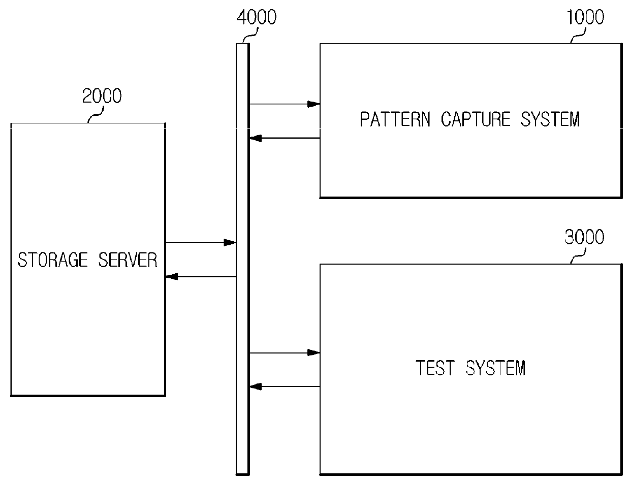
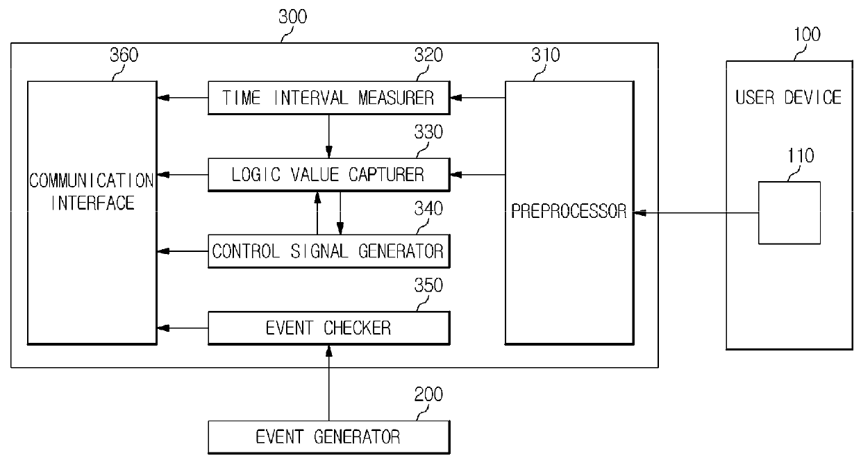
A semiconductor test system includes a user device configured to operate a reference device in accordance with an interface signal based on a timing signal having a variable operating frequency, a pattern synthesis apparatus configured to measure an interval between adjacent edges of the timing signal transmitted from the user device, and extract a logic value of the interface signal in accordance with the timing signal so as to generate test pattern data, and a test device configured to receive the test pattern data, reconstruct the timing signal based on the measured interval, generate a test driving signal such that the logic value is extracted from a device under test (DUT) based on the reconstructed timing signal, and apply the test driving signal to the DUT so as to determine an operating state of the DUT.

Description

CROSS-REFERENCE TO RELATED APPLICATIONS[0001]This application claims priority under 35 U.S.C. §119 to Korean Patent Application No. 2011-0061483, filed on Jun. 24, 2011 in the Korean Intellectual Property Office (KIPO), the entire contents of which are incorporated herein by reference.BACKGROUND[0002]1. Field[0003]Example embodiments of the inventive concepts relate to a pattern synthesis apparatus which determines pass or fail of a semiconductor device, and to a semiconductor test system having the same.[0004]2. Description of the Related Art[0005]Wafers are formed into complete devices through procedures including a fabrication (FAB) process and a subsequent post-process. The thus-formed devices are categorized into non-defective units and defective units by electrical, thermal and functional tests conducted during or after a packaging process. However, a memory module or device which is commercially available after having been determined to be a non-defective unit may not operate...

Claims


Application Information

Patent Timeline
Patent Type & Authority Patents(United States)
IPC IPC(8): G01R31/3183
CPCG01R31/318371G01R31/28
Inventor KIM, SUNG YEOLYANG, IN-SUKIM, MIN SUNGBAEK, JAE HYUNCHOI, JIN-KYUYOO, HO SUN
Owner SAMSUNG ELECTRONICS CO LTD
Why Eureka
Try Eureka