Display panel and demultiplexer circuit thereof

a multi-layer circuit and display panel technology, applied in the field of flat display technology, can solve the problem of easy stress situation, and achieve the effect of reducing time period and reducing the speed of deterioration of transistors

Active Publication Date: 2016-01-26
AU OPTRONICS CORP
View PDF9 Cites 1 Cited by
  • Summary
  • Abstract
  • Description
  • Claims
  • Application Information

AI Technical Summary

Benefits of technology

[0007]The invention and embodiments thereof provide a display panel and a demultiplexer circuit thereof capable of reducing a time period in which transistors in the demultiplexer circuit are in a turned off state so as to mitigate a speed of deterioration for the transistors.
[0016]Based on the above, in the display panel and the demultiplexer circuit of the embodiments of the invention, the control signals are reconfigured as the periods having the first voltage or the second voltage, and the circuit structure of the demultiplexer circuit is correspondingly reconfigured, such that a time length of the transistors in the demultiplexer circuit being turned on is greater than or equal to a time length of being turned off. By this way, stress due to the transistors of the demultiplexer circuit being turned off for a long time can be mitigated.
[0019]Based on the above, the sequence of turning on and off the first to the Nth transistors of the first switch unit of the demultiplexer circuit is adequately configured, such that in follow-up operations of the other switch units, the data line electrically coupled to the first switch unit can be prevented from being provided with wrong signals.

Problems solved by technology

For an N-type TFT, when the TFT is applied with a negative bias voltage for a long time, a stress situation occurs easily.

Method used


Image

  • Display panel and demultiplexer circuit thereof
  • Display panel and demultiplexer circuit thereof
  • Display panel and demultiplexer circuit thereof

Examples


Embodiment Construction

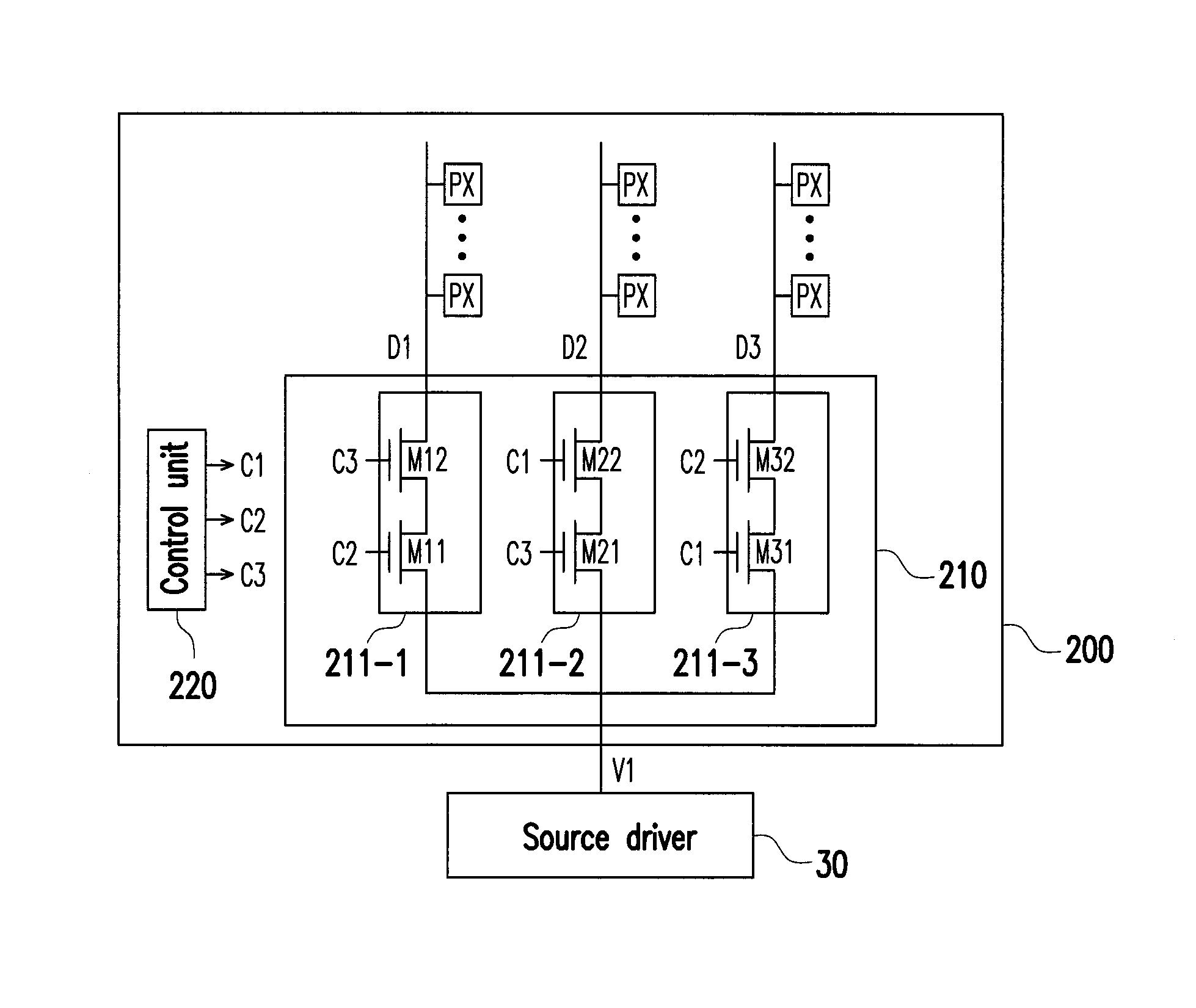
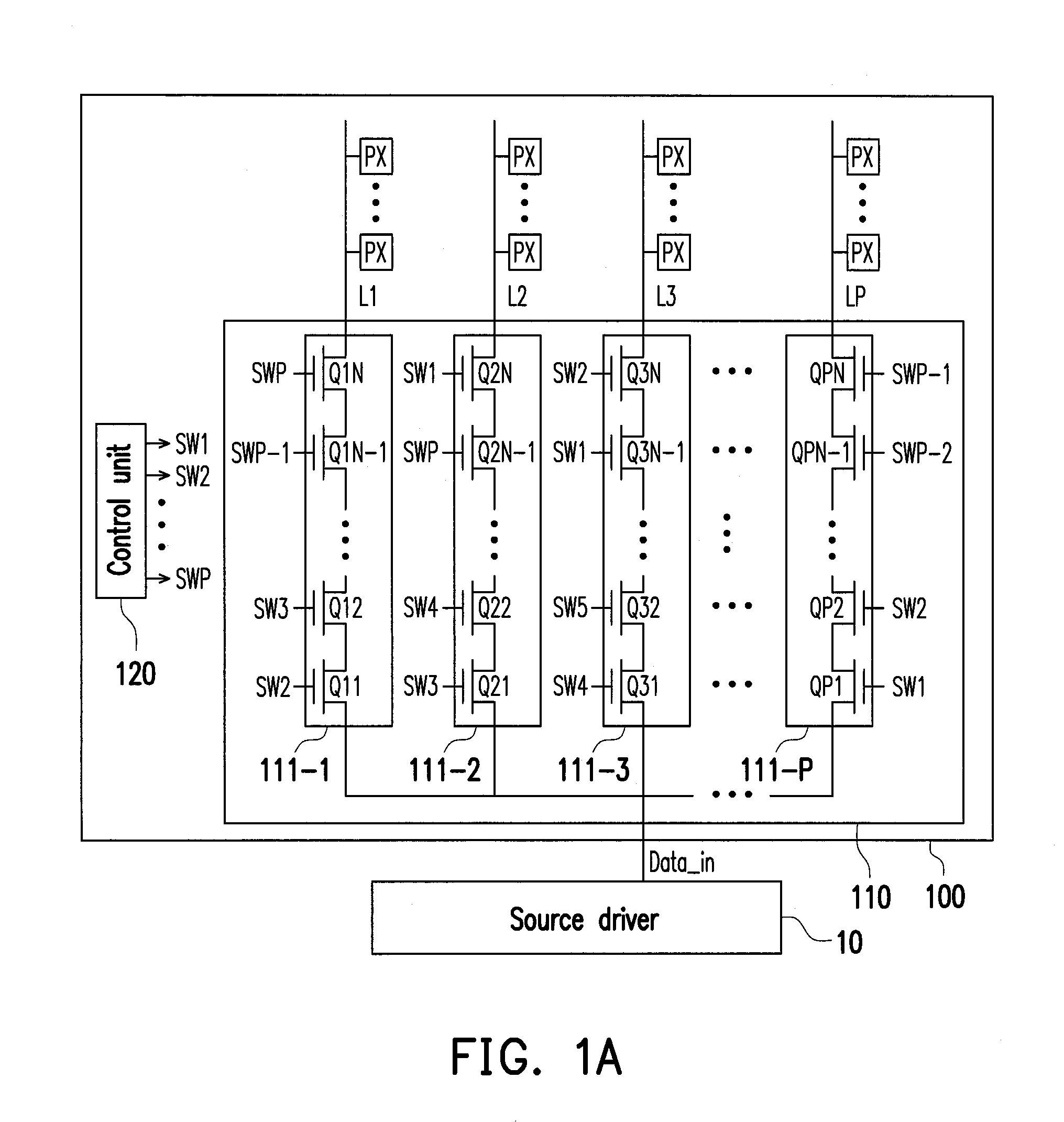
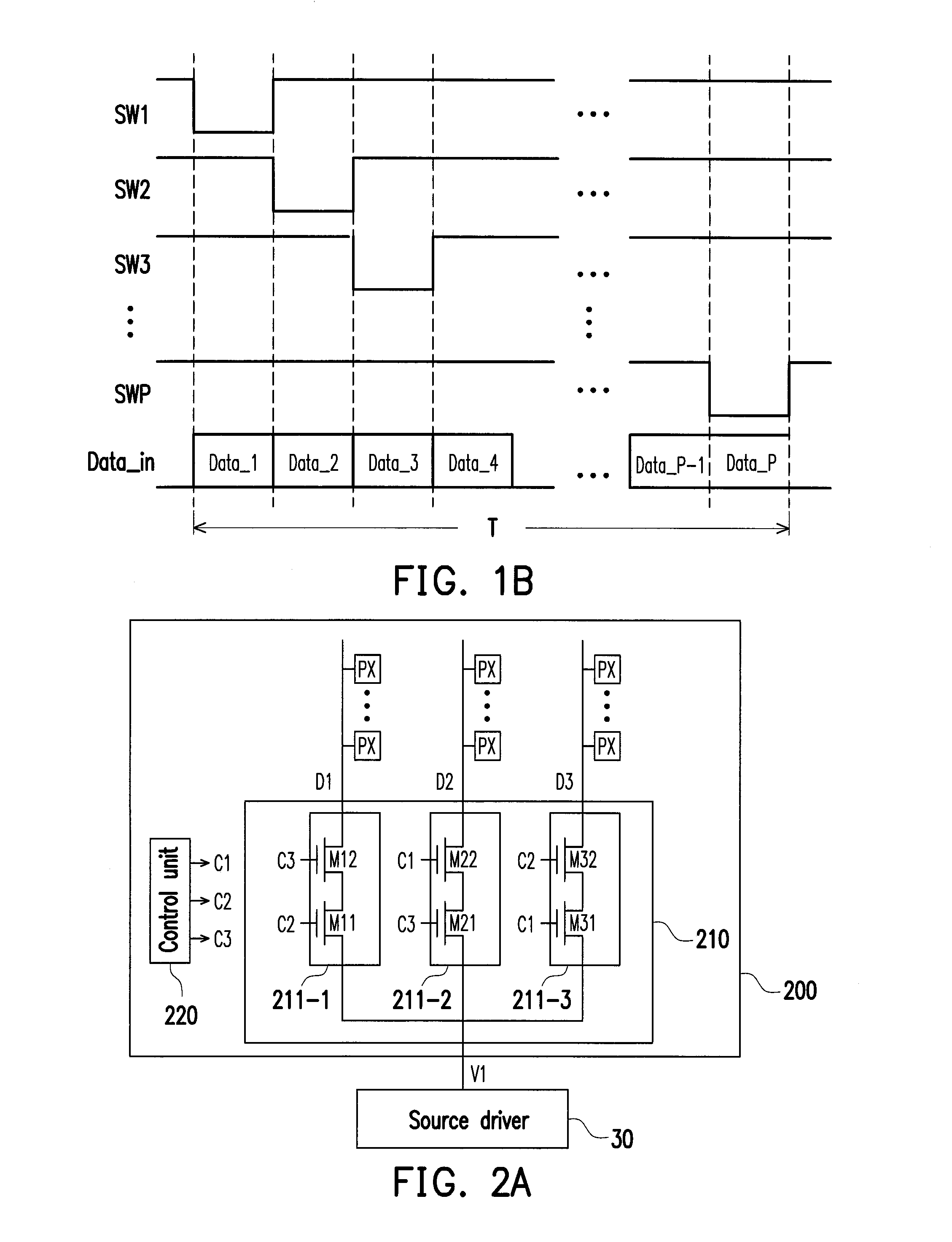
[0029]FIG. 1A is a schematic circuit diagram illustrating a display panel according to an embodiment of the invention. FIG. 1B is a schematic diagram illustrating a drive waveform of the demultiplexer circuit depicted in FIG. 1A. Description with reference to FIG. 1A and FIG. 1B will be set forth below. In the present embodiment, a display panel 100 includes a plurality of pixels PX, a plurality of data lines L1 to LP, a demultiplexer circuit 110 and a control unit 120. The data lines L1 to LP are electrically coupled to the corresponding pixels PX respectively, and the demultiplexer circuit 110 is electrically coupled to the data lines L1 to LP. The demultiplexer circuit 110 is configured to transmit a data voltage Data_in provided by the source driver 10 to the data lines L1 to LP, and the control unit 120 is configured to generate a plurality of control signals SW1 to SWP (corresponding to a first to a Pth control signals) to control a transmission state of the demultiplexer circ...


PUM


Abstract

A display panel and a demultiplexer circuit are provided. The demultiplexer circuit includes a first to a Pth switch units. The first to the Pth switch units are coupled to a first to a Pth data lines of a display panel respectively and collectively receive a data voltage and turn on sequentially in sequence to provide the data voltage to corresponding data lines. A period of the first to the Pth switch units provide the data voltage to the first to the P data lines sequentially which is defined to a data transmission period. When the switch unit is turned on, N transistors are turned on simultaneously according to a plurality of control signals. When the switch unit is turned off, at least one of the N transistors is turned off according to a corresponding control signal.

Description

CROSS-REFERENCE TO RELATED APPLICATION[0001]This application claims the priority benefit of Taiwan application serial no. 103103589, filed on Jan. 29, 2014. The entirety of the above-mentioned patent application is hereby incorporated by reference herein and made a part of this specification.BACKGROUND[0002]1. Field of the Invention[0003]The invention is related to a flat display technology and more particularly, to a display panel and a demultiplexer circuit thereof.[0004]2. Description of Related Art[0005]With progress in manufacturing technologies of semiconductors, volumes of various types of electronic products are also developed toward being light and thin. In other to meet demands for miniaturization of the electronic products, flat panel displays are widely used due to having advantages, such as good space utilization efficiency, high definition, low power consumption, radiation free and so on. Generally, a flat panel display includes elements, such as a backlight module, a ...

Claims


Application Information

Patent Timeline
Patent Type & Authority Patents(United States)
IPC IPC(8): G09G5/00G09G3/32G09G3/36G09G3/20G09G3/3275
CPCG09G3/2096G09G3/3275G09G3/3685G09G2310/0213G09G2310/0297G09G2320/043
Inventor LIN, CHEN-CHICHANG, CHIH-HSIANG
Owner AU OPTRONICS CORP
Why Eureka
Try Eureka