
Focus control apparatus and method

a control apparatus and focus technology, applied in the field of focus control apparatus, can solve the problems of deteriorating the degree of precision the great error of the real focus error, and the deterioration of the focus position control so as to reduce the degree of precision of surface inspection in proximity to the interface, improve the response characteristics of the focus error signal, and improve the effect of the focus position control

Active Publication Date: 2016-02-09
SAMSUNG ELECTRONICS CO LTD
View PDF2 Cites 0 Cited by
  • Summary
  • Abstract
  • Description
  • Claims
  • Application Information

AI Technical Summary

Benefits of technology

[0019]Further, in FIG. 12, response characteristics of the focus error signal can be improved within an allowable range of the stage control mechanism 107 for moving the XYZ stage 104 having the semiconductor wafer 105 mounted thereon.
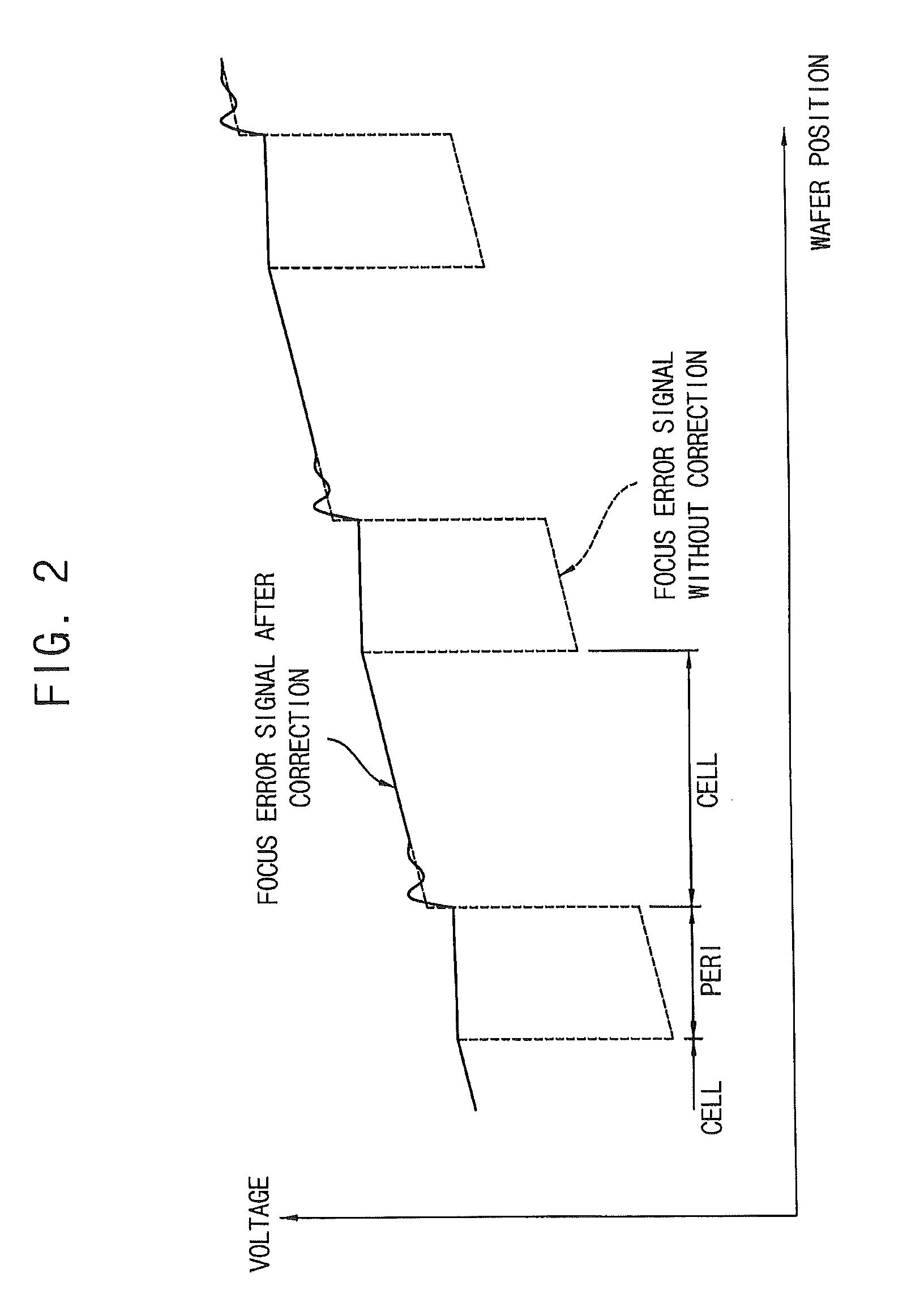
[0020]However, when one of the peripheral region 105P and the cell region 105C is changed to the other, a transient response occurs due to a rapid change of the signal intensity near the step portion therebetween. Accordingly, for a while after the region is changed, the focus error signal cannot follow the real focus position error to thereby deteriorate the degree of the focus position control in proximity to the interface. Thus, the degree of precision of a surface inspection in proximity to the interface is decreased.
[0021]Example embodiments provide a focus control apparatus and method capable of generating a focus position signal according to a real focus position error even in proximity to the interface between regions having different thicknesses to perform a high precision focus position control using the focus position signal.

Problems solved by technology

However, in case the focus error signal of FIG. 11 is used, the focus error signal near the interface between the peripheral region 105P and the cell region 105C has a great error from the real focus error, due to smoothing of the low pass filter.
As a result, the focus error signal near the interface having the error is used for the focus position control, thereby deteriorating the degree of precision of the focus position control in proximity to the interface.
Accordingly, the degree of the focus position control in proximity to the interface is deteriorated and thus the degree of precision of a surface inspection in proximity to the interface is decreased.
Accordingly, for a while after the region is changed, the focus error signal cannot follow the real focus position error to thereby deteriorate the degree of the focus position control in proximity to the interface.

Method used


Image

  • Focus control apparatus and method
  • Focus control apparatus and method
  • Focus control apparatus and method

Examples


first example embodiment

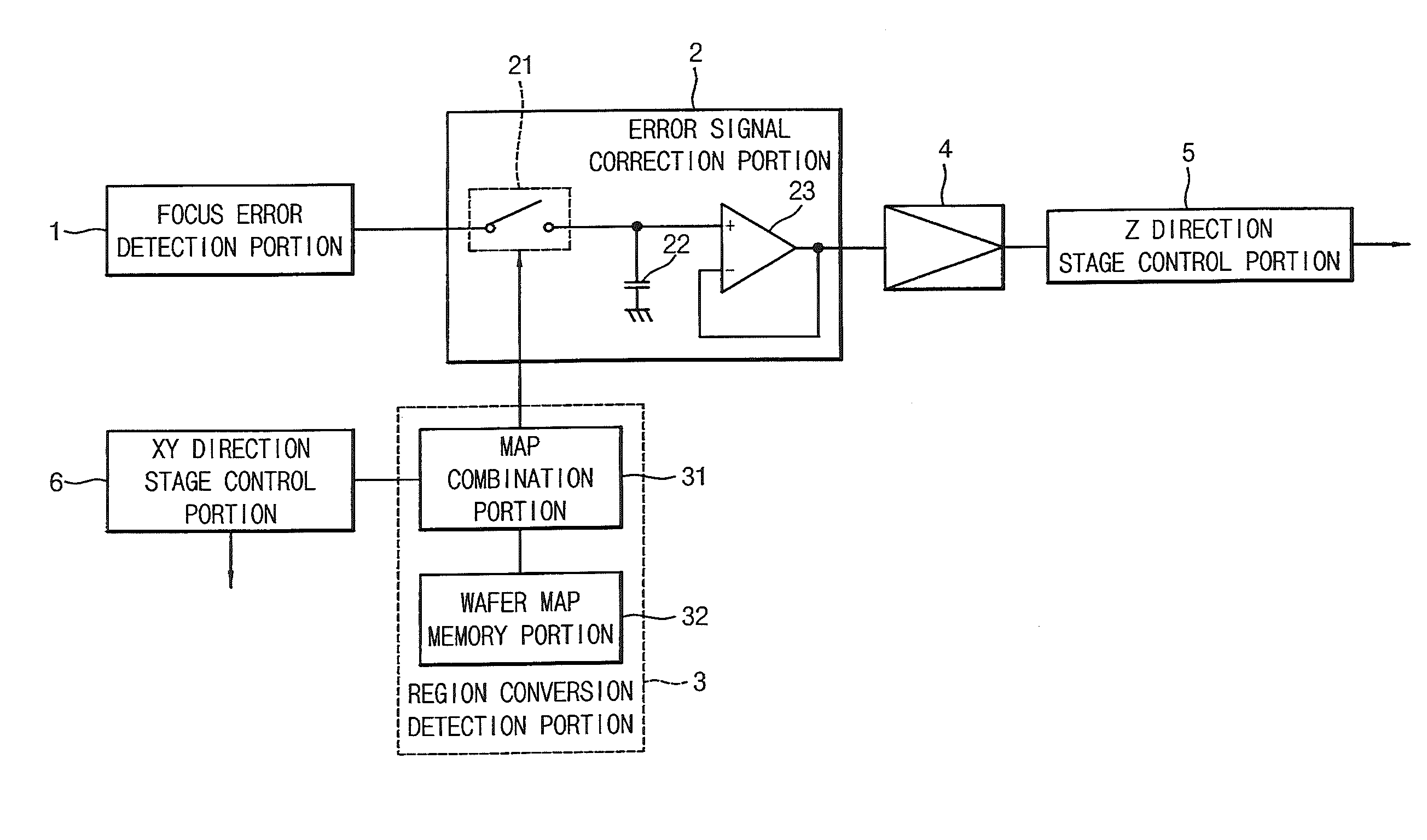
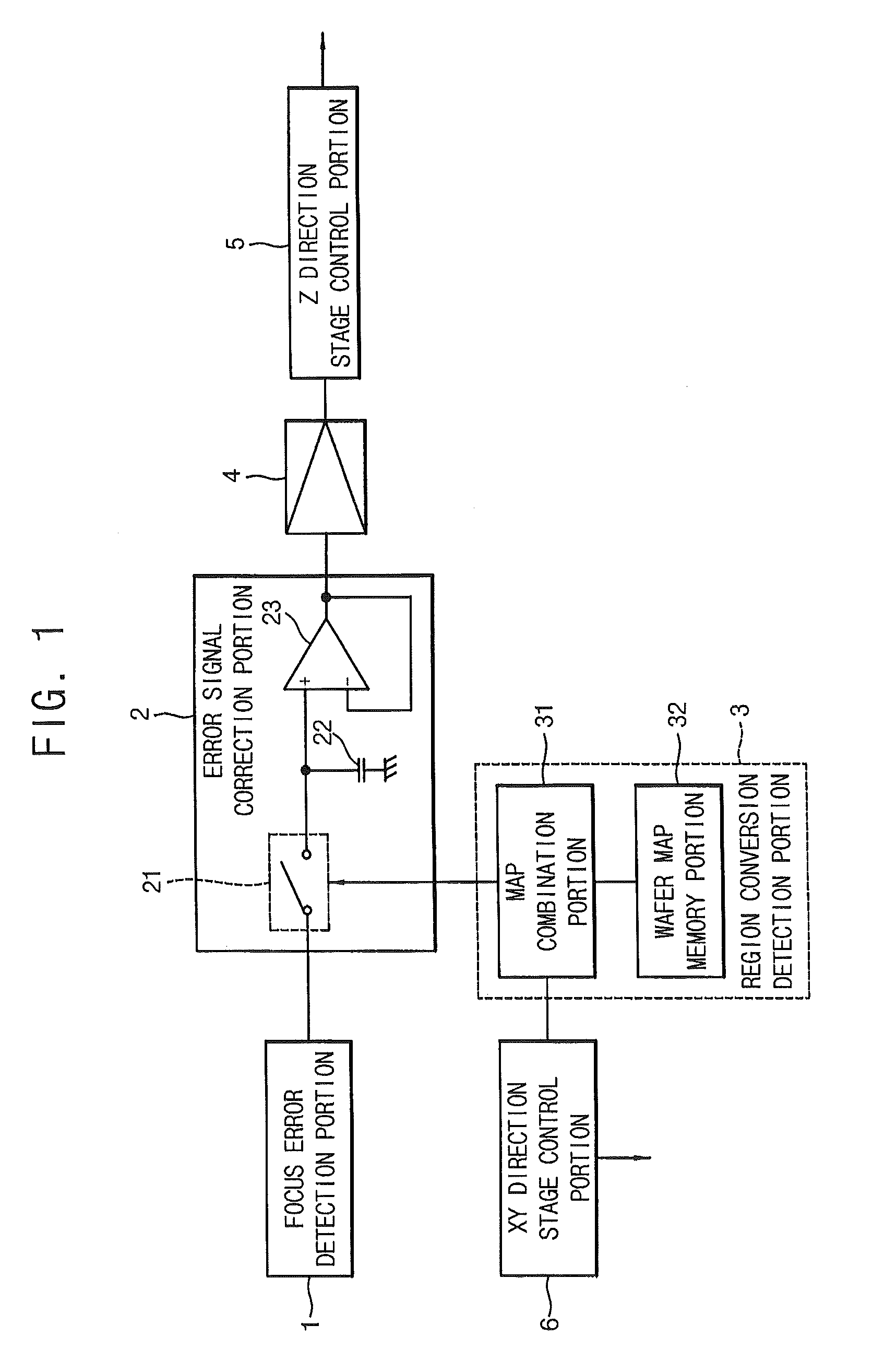
[0041]Hereinafter, a first example embodiment will be explained in detail with reference to the accompanying drawings. FIG. 1 is a block diagram illustrating a construction of a focus control apparatus in accordance with a first example embodiment. Hereinafter, a construction of the focus control apparatus according to a first example embodiment which is substituted for the focus position control portion 106 of a semiconductor inspecting apparatus including a microscope, which performs a surface inspection of the semiconductor wafer 105, will be explained.

[0042]The focus control apparatus according to this example embodiment includes a focus error detection portion 1, an error signal correction portion 2, a region conversion detection portion 3, a driver4, a Z direction stage control portion 5, and an XY direction stage control portion 6.

[0043]The focus error detection portion 1 changes a deviation amount of a focus position with respect to a surface of the semiconductor wafer 105 o...

second example embodiment

[0060]Hereinafter, a second example embodiment will be explained with reference to the accompanying drawings. FIG. 3 is a block diagram illustrating a focus control apparatus in accordance with a second example embodiment. Hereinafter, a construction of the focus control apparatus according to a second example embodiment which is substituted for the focus position control portion 106 of a semiconductor inspecting apparatus performing a surface inspection of the semiconductor wafer 105 will be explained.

[0061]The focus control apparatus according to this example embodiment includes a focus error detection portion 1, an error signal correction portion 2A, a region conversion detection portion 3, a driver 4, a Z direction stage control portion 5, and an XY direction stage control portion 6. The focus control apparatus according to this example embodiment is substantially the same as in the first example embodiment except the error signal correction portion 2A. Thus, a construction and ...


PUM


Abstract

A focus control apparatus and method capable of generating a focus position signal according to focus position error even in proximity to an interface between regions having different thicknesses, to perform a high precision focus position control using the focus position signal, are provided. A focus control apparatus includes an error signal correction portion configured to process a focus error signal that indicates an error of a focus position of an optical system with respect to an object. Moreover, the focus control apparatus includes a region conversion detection portion configured to output a region signal that corresponds to a first region or a second region of the object. The first and second regions of the object have different respective heights.

Description

CROSS-REFERENCE TO RELATED APPLICATION[0001]This application claims priority under 35 U.S.C. §119 to Japanese Patent Application No. 2012-267407, filed on Dec. 6, 2012 in the Japan Patent Office, the contents of which are herein incorporated by reference in their entirety.BACKGROUND[0002]1. Field[0003]Example embodiments relate to a focus control apparatus for controlling a focus in an optical system of a microscope.[0004]2. Description of the Related Art[0005]In order to perform a surface inspection of a semiconductor device, an optical semiconductor inspecting apparatus includes a microscopic system having a high precision automatic focus control performance to optically form an image from a fine pattern (for example, see Patent document 1). FIG. 8 is a view illustrating a general optical semiconductor inspecting apparatus. A light illumination portion 101 emits a light toward an optical system 102 of a microscope. Then, the light from the light illumination portion 101 is inciden...

Claims


Application Information

Patent Timeline
Patent Type & Authority Patents(United States)
IPC IPC(8): G02B21/26G02B21/24G02B21/00
CPCG02B21/26G02B21/247G02B21/0016
Inventor TOGASHI, MITSUHIROSEKIYA, HARUTAKA
Owner SAMSUNG ELECTRONICS CO LTD
Learn More