Wafer carrier

a carrier and wafer technology, applied in the field of wafer carriers, can solve the problems of increasing weight, increasing fragility, increasing cost, etc., and achieving the effects of reducing cost, enhancing performance, and easy and robust and precise attachmen

Active Publication Date: 2016-04-12
ENTEGRIS INC
View PDF15 Cites 9 Cited by
  • Summary
  • Abstract
  • Description
  • Claims
  • Application Information

AI Technical Summary

Benefits of technology

[0012]A front opening wafer container comprising a container portion and door particularly for large diameter wafers 300 mm and greater, particularly for 450 mm wafers, utilizes componentry with separate fasteners to lock the componentry together in an expedient manner providing robust connections and cost efficiencies. A container portion has an open front and receives on a bottom surface a base plate secured by twist lock connectors that also provide recesses for purge grommets. Kinematic coupling components readily and robustly lock onto the base plate. Interior wafer support components latch with brackets on the side walls and utilize a separate locking insert with holding tabs and locking detents. A wafer retainer provides support and counters enhanced wafer sag associated with 450 mm wafers when the door is installed and seated.
[0016]Additionally, a base plate with kinematic couplings may also be secured utilizing additional fastener components including twist lock connectors that provides a robust connection of the base plate with minimal assembly, minimal particle generation, and allows use of the connections as purge ports. The base plate may utilize snap-in kinematic coupling components that readily and robustly and precisely attach to conforming apertures on the base plate. Again the connector secures the two principal components in engagement with one another such that the load transfer between the two components does not substantially extend through the connecter securing the components.
[0017]Thus, a wafer container suitable for use with large wafers, including 450 mm wafers is presented with novel component configuration and attachment means. Said novelty provides enhanced performance, manufacturing expedience and reduced cost.

Problems solved by technology

Such intra-facility and extra-facility movements may generate or expose the wafers to potential wafer ruining contaminants.
The larger diameter wafers, although providing cost efficiencies, also provide increased fragility, greater weight, and present undiscovered issues associated with handling and storing the larger wafers in containers made of plastic.
Assembly of larger components and the manufacturing tolerances of the components being assembled are more problematic.
Forces exerted by the increased weight of substrates on the larger components cause more stress, manufacturing tolerances are greater and conventional connection techniques between components may be inadequate or not optimum.
When dealing with greater weights and larger components such configurations may not be optimal.
Wafers of larger dimensions also have significantly greater sag which will make them more susceptible to damage during handling and transport and require unique support not required for smaller wafers.
This greater sag presents challenges in maintaining the desired spacing between wafers while still allowing placement and removal of the wafers robotically by robotic arms.
With the greater sag associated with 450 mm wafers, conventional ramps as illustrated in U.S. Pat. No. 6,010,008 may not be optimal.
Along with increasing size of semiconductor wafers, the density of the circuits formed on the wafers has also been increasing, making the circuits more susceptible to defects from smaller and smaller particles and other contaminants.
In short, as wafers have increased in size, containers have increased in size as well, and the requirements for keeping the wafers clean and contaminant free have become more stringent due to the wafers being more susceptible to smaller particles and other contaminants.

Method used


Image

  • Wafer carrier
  • Wafer carrier
  • Wafer carrier

Examples


Embodiment Construction

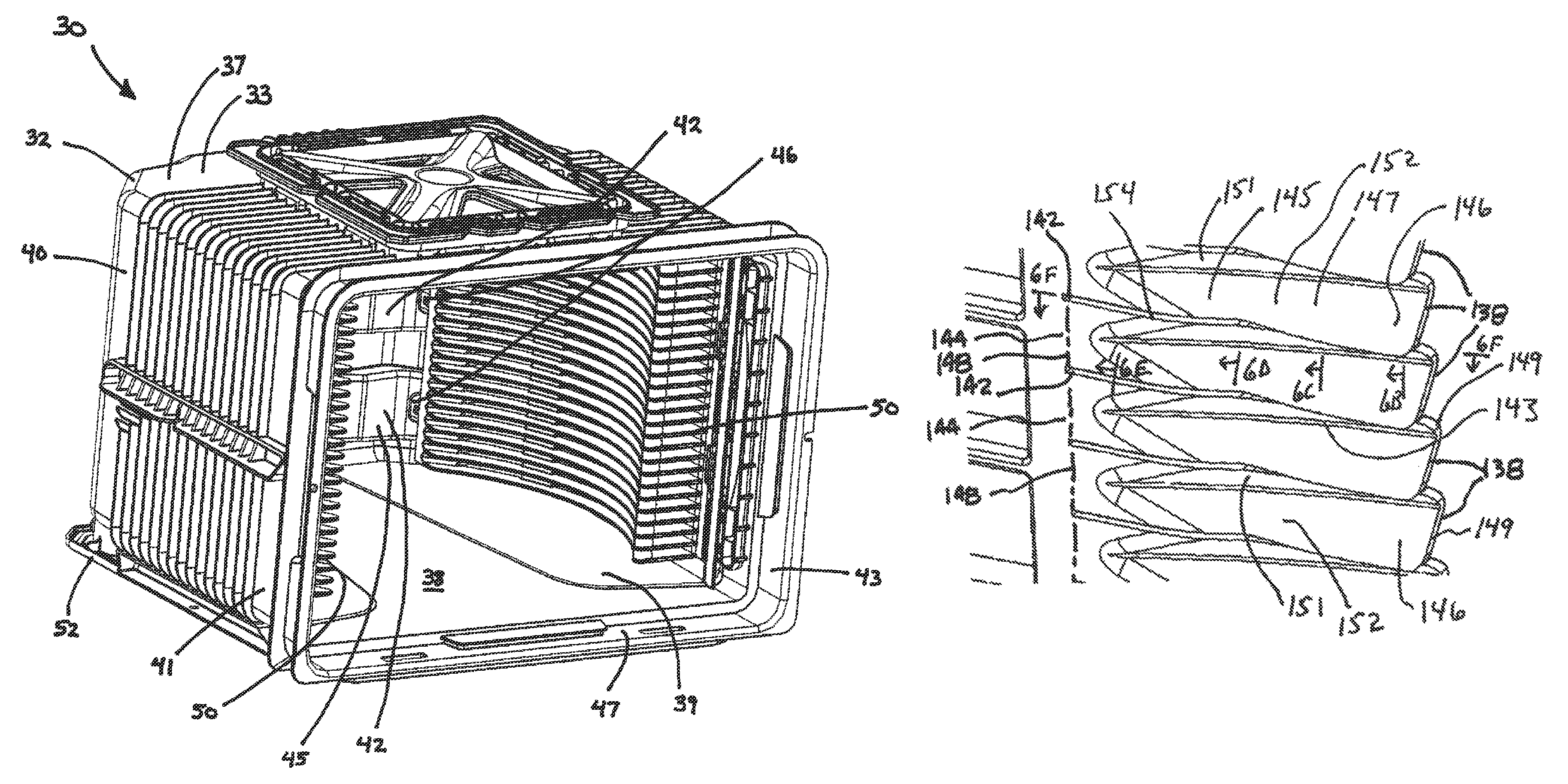
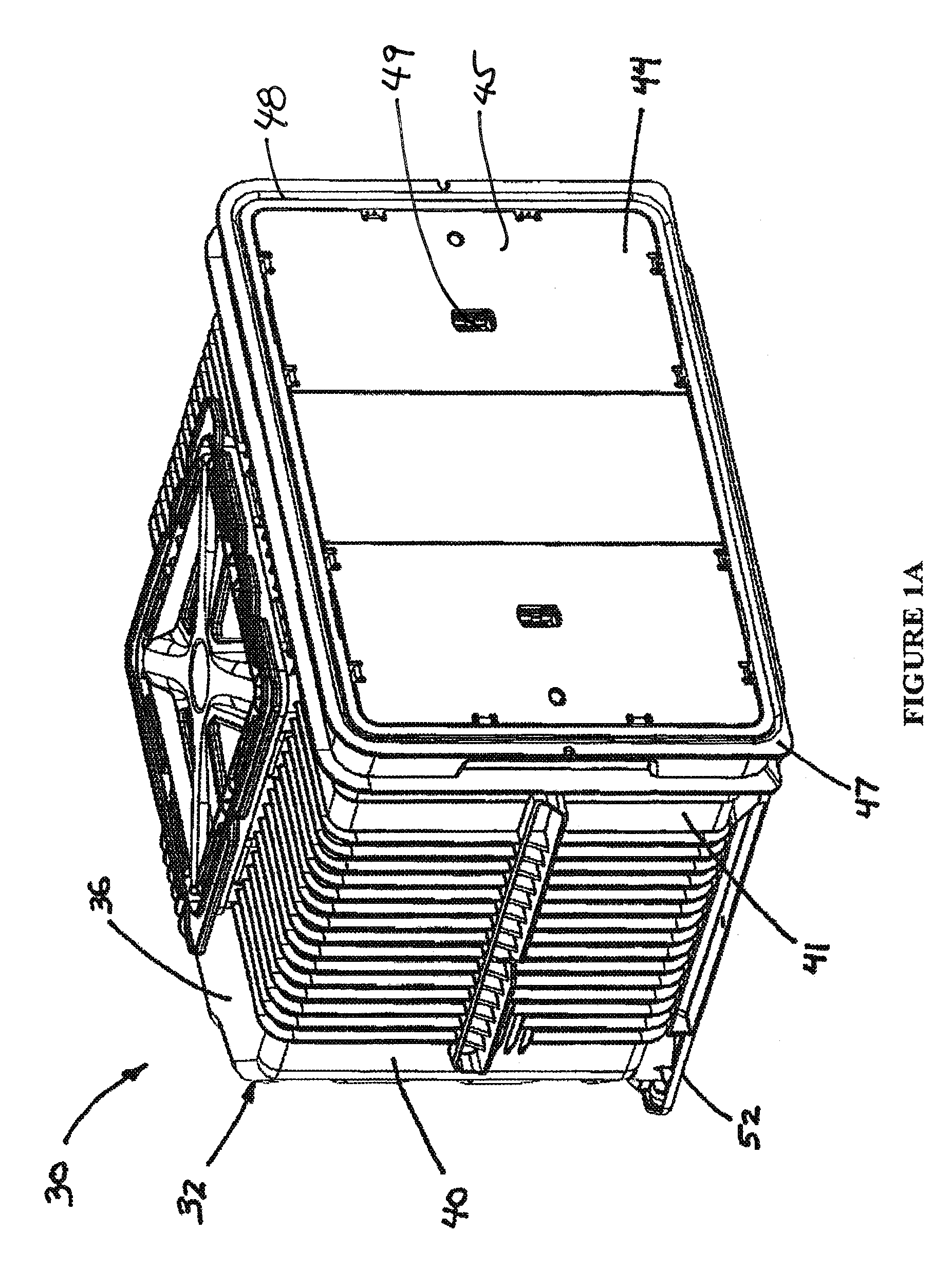
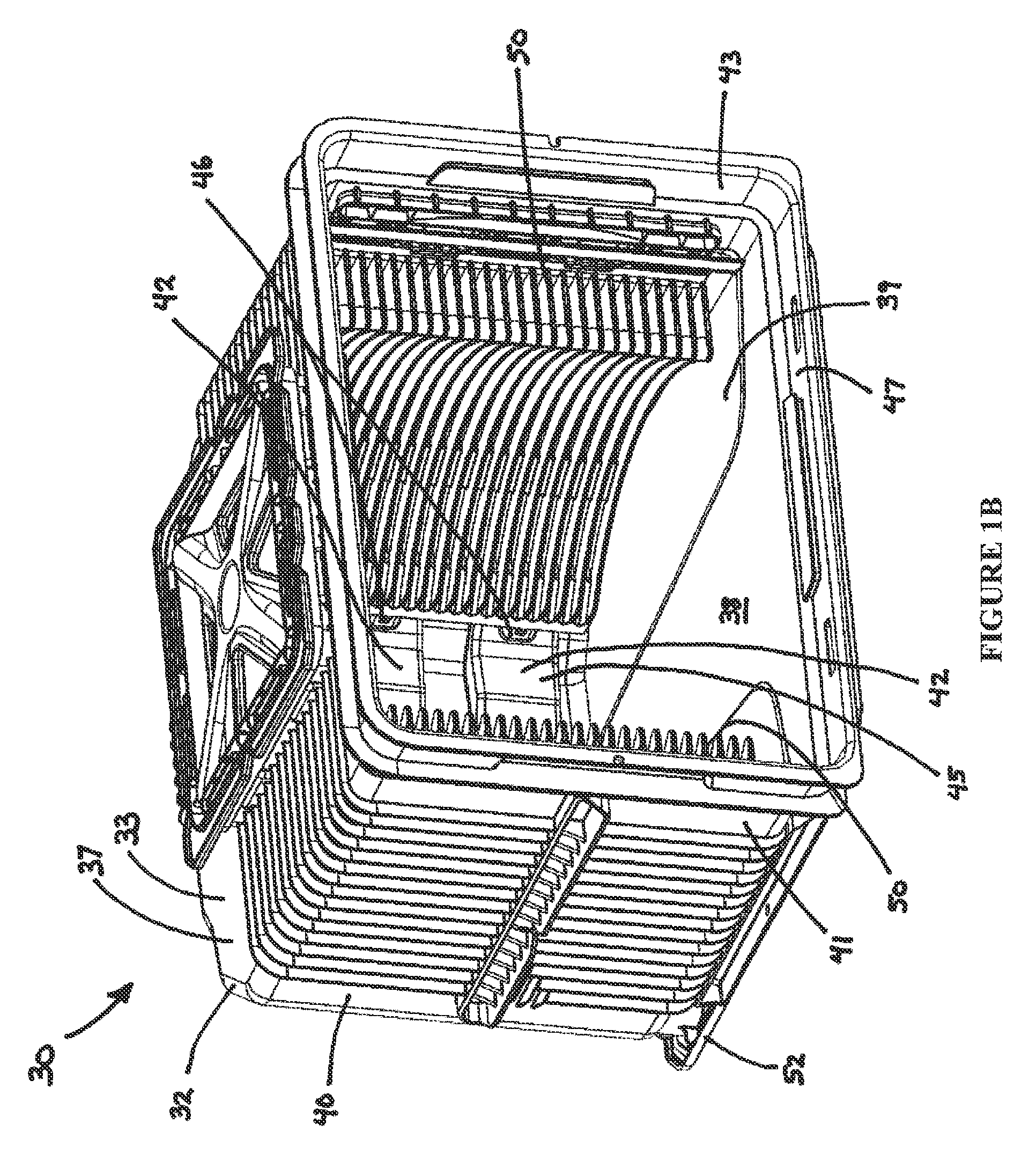
[0051]Referring to FIGS. 1A, 1B and 1C, a multiple application carrier (MAC) 30 is depicted in an embodiment of the invention. The MAC 30 comprises a container portion 32 generally having a shell 33 including an upper portion 36, a top wall 37, a lower portion 38, a bottom wall 39, two side portions 40, two side walls 41, a back wall 42, and a back portion 45. The upper portion 36, lower portion 38 and the two side portions 40 extent toward a front opening 43 configured as a door frame 47 that can be closed and sealed with a door 44 having an outside facing surface 45, a periphery 48, and a latching mechanism 49. In one embodiment, the back portion 42 of the container portion 32 includes a plurality of brackets 46 configured as mounting pockets formed thereon. A pair of wafer support components 50 each have a pair of integrally molded cooperating brackets. The brackets cooperate with brackets on the shell. A locking clip may secure the wafer support component in place. A base plate ...


PUM


Abstract

A front opening wafer container suitable for large wafers such as 450 mm utilizes componentry with separate fasteners to lock the componentry together in an expedient manner providing robust connections and cost efficiencies. A container portion has an open front and receives on a bottom surface a base plate secured by twist lock connectors that also provide recesses for purge grommets. Kinematic coupling components readily and robustly lock onto the base plate. Interior wafer support components latch onto brackets on the side walls utilizing a separate locking insert with holding tabs and locking detents. A wafer retainer provides support and counters enhanced wafer sag associated with 450 mm wafers when the door is installed and seated.

Description

PRIORITY CLAIM[0001]The present application is a National Phase entry of PCT Application No. PCT / US2012 / 050624, filed Aug. 13, 2012, which claims priority to U.S. Provisional Patent Application No. 61 / 523,254, filed Aug. 12, 2011, the disclosures of which are hereby fully incorporated by reference in their entirety.FIELD OF THE INVENTION[0002]This invention relates to containers for sensitive substrates such as semiconductor wafers and in particular to components and assembly of the components into such containers.BACKGROUND OF THE INVENTION[0003]Integrated circuits such as computer chips are manufactured from semiconductor wafers. These wafers are subjected to numerous steps during the process of making integrated circuits. This generally entails transporting a plurality of wafers from one workstation to another for processing by specialized equipment. As part of the processing procedure, wafers may be temporarily stored or shipped in containers to other plants or to end users. Suc...

Claims


Application Information

Patent Timeline
Patent Type & Authority Patents(United States)
IPC IPC(8): H01L21/673
CPCH01L21/67379H01L21/67369H01L21/67373H01L21/67376H01L21/67383H01L21/67386H01L21/673H01L21/67303H01L21/67389
Inventor ADAMS, MICHAEL S.GREGERSON, BARRYFULLER, MATTHEW A.
Owner ENTEGRIS INC
Why Eureka
Try Eureka