Semiconductor package and lidar transmission unit

A semiconductor and surface emission technology, applied in the direction of semiconductor devices, semiconductor lasers, semiconductor/solid-state device components, etc., can solve problems such as high cost

Pending Publication Date: 2020-11-10
IBEO AUTOMOTIVE SYST
View PDF1 Cites 0 Cited by
  • Summary
  • Abstract
  • Description
  • Claims
  • Application Information

AI Technical Summary

Problems solved by technology

In cases where at least the resolution of a surface-emitting laser is required, the minimum size of the laser is therefore predetermined, which leads to high costs for semiconductor manufacturing, since the semiconductor surface itself increases as well as the error rate for larger semiconductor components the next time products, resulting in higher cost

Method used


Image

  • Semiconductor package and lidar transmission unit
  • Semiconductor package and lidar transmission unit
  • Semiconductor package and lidar transmission unit

Examples


Embodiment Construction

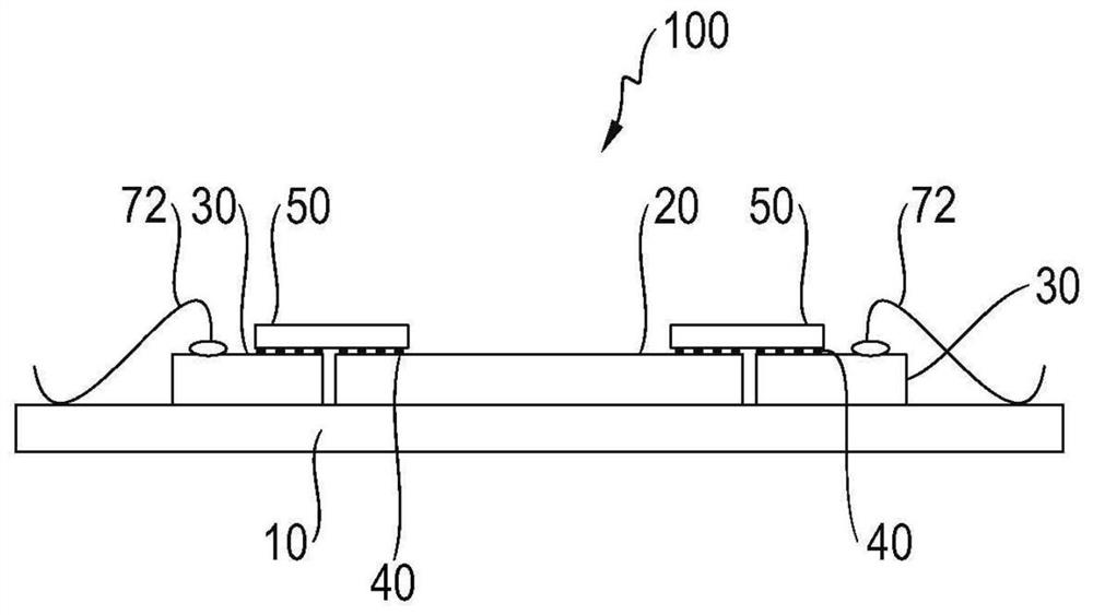
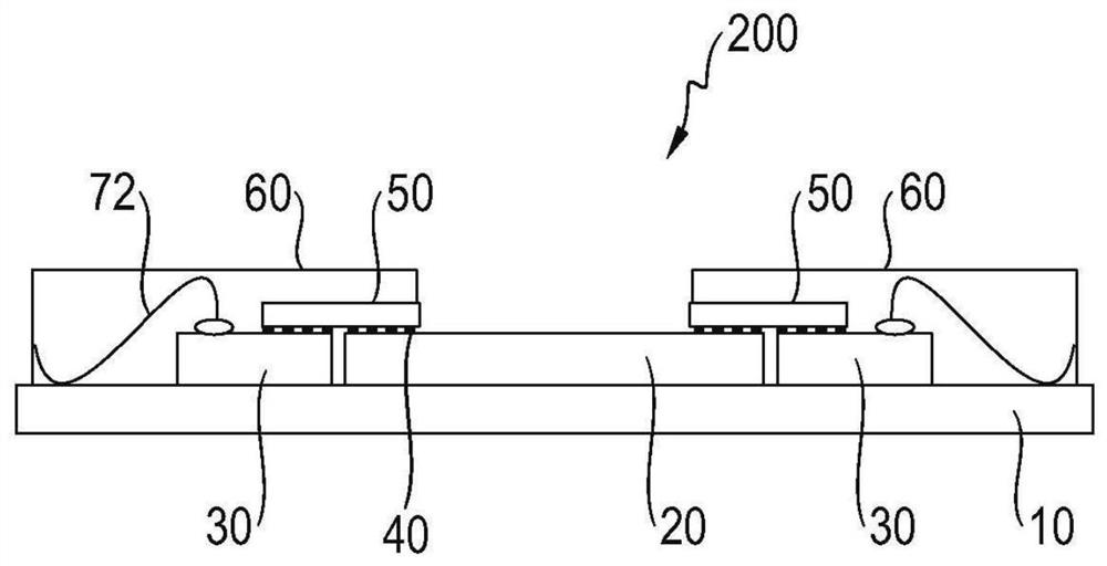
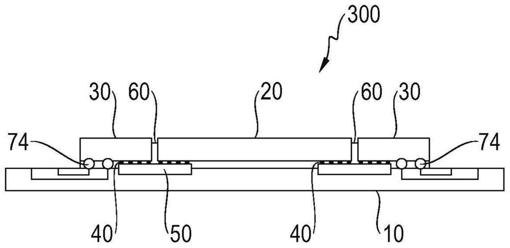
[0029] Exemplary embodiments will now be described in detail with reference to the accompanying drawings that illustrate some exemplary embodiments. In the following description of the drawings showing only some exemplary embodiments, the same reference numerals may denote the same or comparable components. Furthermore, collective reference numbers may be used for components and objects that appear multiple times in one exemplary embodiment or in one figure but are commonly described with respect to one or more features. In this case, the vertical extension or vertical arrangement is defined as normal to the front surface of the packaging substrate and the lateral extension or lateral arrangement is defined as parallel to the front surface of the packaging substrate.

[0030] figure 1 An exemplary embodiment of a semiconductor package is shown. The semiconductor package 100 includes a package substrate 10 , a surface emitting laser 20 , two driver circuits 30 for the surface...


PUM

PropertyMeasurementUnit
diameteraaaaaaaaaa

Abstract

The present invention relates to a semiconductor package and to a LIDAR transmitting unit comprising such a semiconductor package. The semiconductor package comprises a surface-emitting laser, at least one driver circuit for the surface-emitting laser, a connecting structure and at least one interposer. The connecting structure comprises a plurality of solder bumps. The surface-emitting laser is electrically connected to the at least one driver circuit via the at least one interposer and the connecting structure.

Description

technical field [0001] The present invention relates to a semiconductor package, more particularly to a semiconductor package comprising a surface emitting laser, at least one driver circuit for the surface emitting laser and at least one interposer, and a LIDAR emitting unit comprising such a semiconductor package. Background technique [0002] In laser array devices, such as LIDAR applications (Light Detection and Ranging, Light-Based Detection and Distance Measurement), surface-emitting lasers, so-called VCSELs (Vertical Cavity Surface-Emitting Lasers, surface-emitting lasers with vertical resonators) are often used ). These surface emitting lasers are arranged on a semiconductor package together with corresponding driver circuits. In this case, usually the electrical contact between the driver circuit and the surface emitting laser is made via bonding wires. [0003] In some applications, such as in the automotive field, such bonding wires have a distance (also called ...

Claims


Application Information

Patent Timeline
Patent Type & Authority Applications(China)
IPC IPC(8): H01S5/026H01S5/18G01S7/481G01S7/484
CPCH01S5/0261H01S5/18G01S7/4815G01S7/484H01S5/183G01S7/481H01L2224/16227H01L2224/1703H01L2924/15192H01L2924/15311H01L2224/73204H01L2224/32225H01L2224/92125H01L2924/18161H01L2224/131H01L2224/48227H01L2224/73265H01L2224/48465H01L2224/73207H01L2224/73253H01L2924/1815H01L2224/48091H01L24/13H01L24/16H01L24/17H01L24/32H01L24/48H01L24/73H01L24/92H01S5/02234H01S5/02325H01S5/0237H01S5/02345H01L2924/014H01L2924/00014H01L2924/00012H01L2224/16225H01L2924/00H01L23/48H01L24/10H01L24/42H01L24/97H01L23/488H01L24/14G01S7/4808G01S7/4813G01S7/4861
Inventor S·哈克斯皮耶尔
Owner IBEO AUTOMOTIVE SYST
Why Eureka
Try Eureka