Method for manufacturing array substrate

a technology of array substrates and manufacturing methods, which is applied in the direction of basic electric elements, electrical equipment, semiconductor devices, etc., can solve the problems of high cost and complicated processing of ltps array substrates, and achieve the effect of less manufacturing processes and cost reduction

Active Publication Date: 2016-04-12
TCL CHINA STAR OPTOELECTRONICS TECH CO LTD
View PDF4 Cites 0 Cited by
  • Summary
  • Abstract
  • Description
  • Claims
  • Application Information

AI Technical Summary

Benefits of technology

[0008]The present invention is to propose a method for manufacturing an array substrate. The manufacturing method facilitates reduction of use of mask plates, thereby reducing production cost. The manufacturing method is suitable to manufacture a-Si array substrates of low-definition OLED display panels.
[0072]Only four masks are conducted in the embodiment of the present invention. The a-Si array substrates of low-definition OLED display panels undergo less manufacturing processes, which means that mask plates are used less and cost is reduced.

Problems solved by technology

It is more complicated to process LTPS array substrates.
However, it is not recommendable that amorphous silicon (a-Si) array substrates of low-definition (LD) panels undergo 9 to 13 masks that LTPS array substrates undergo since the processes are complicated and cost is high.

Method used


Image

  • Method for manufacturing array substrate
  • Method for manufacturing array substrate
  • Method for manufacturing array substrate

Examples


Embodiment Construction

[0079]The accompanying drawings are included to provide a further understanding of the invention. The drawings illustrate embodiments of the invention and, together with the description, serve to explain the principles of the invention.

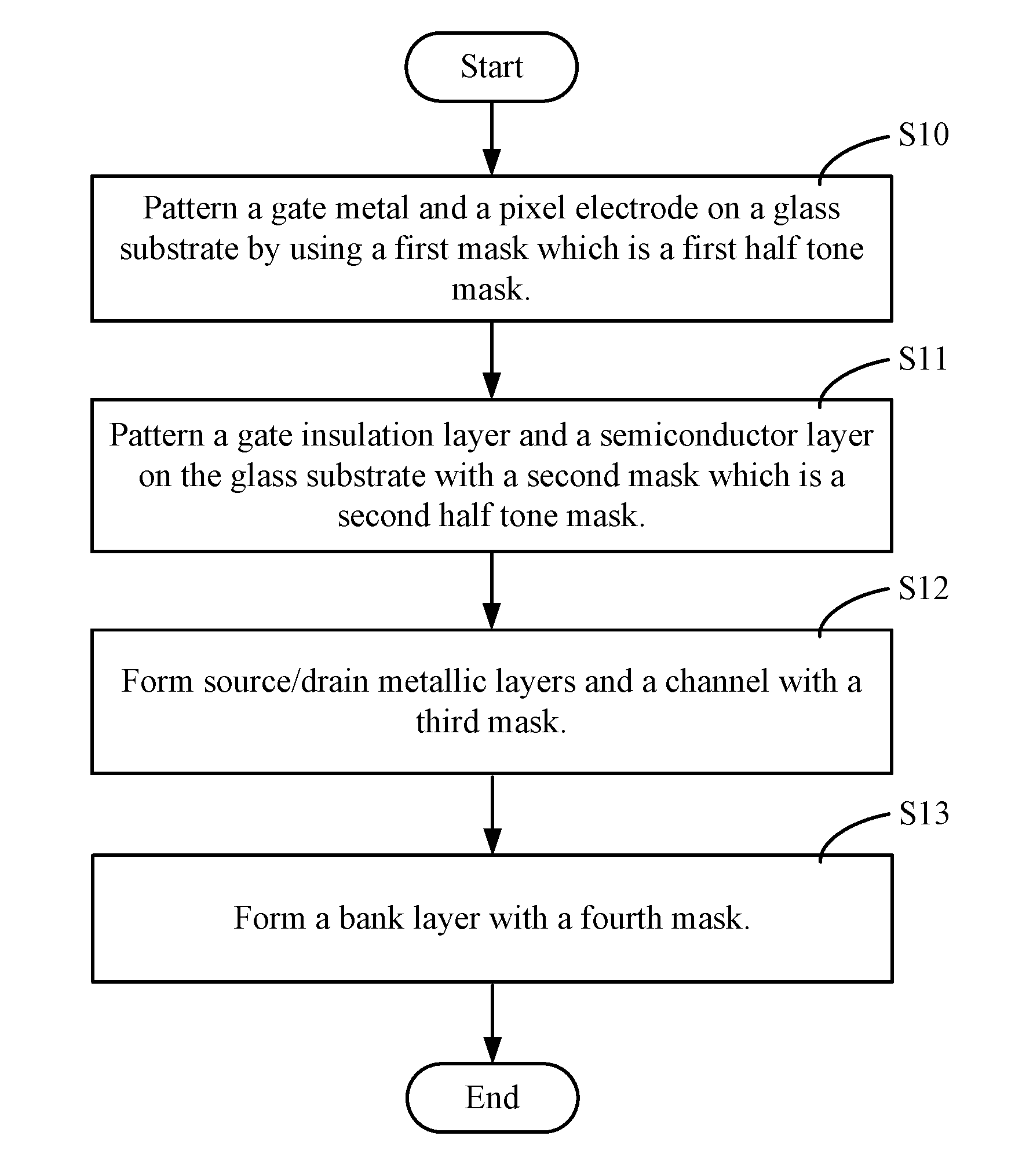
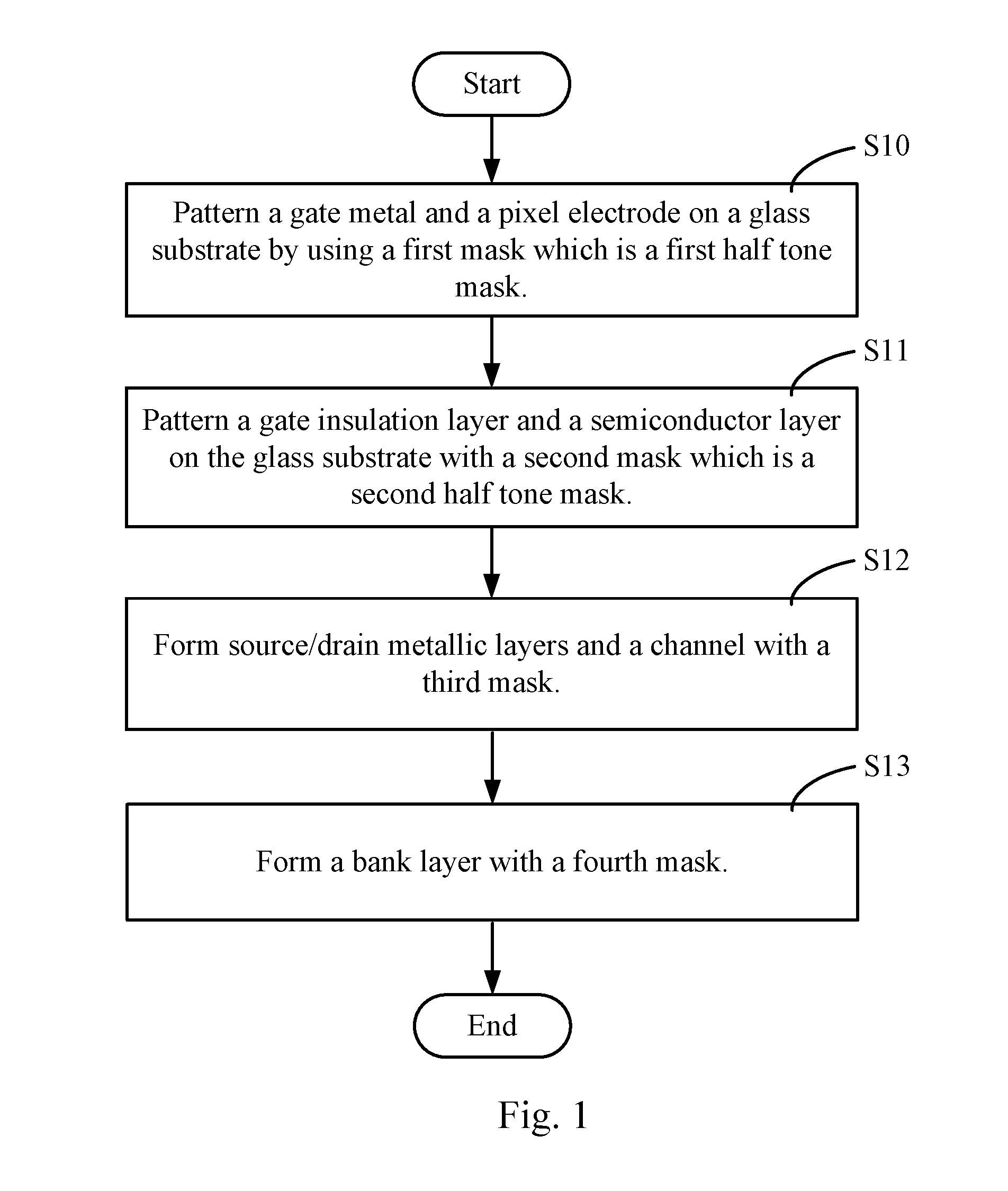
[0080]Refer to FIG. 1 showing a flow chart of a method for manufacturing an array substrate according one embodiment of the present invention. An a-Si array substrate of a low-definition OLED display panel can be produced with the method proposed by the embodiment. The method comprises following steps:

[0081]Step S10: patterning a gate metal and a pixel electrode on a glass substrate with a first mask which is a first half tone mask.

[0082]Specifically, the step comprises:

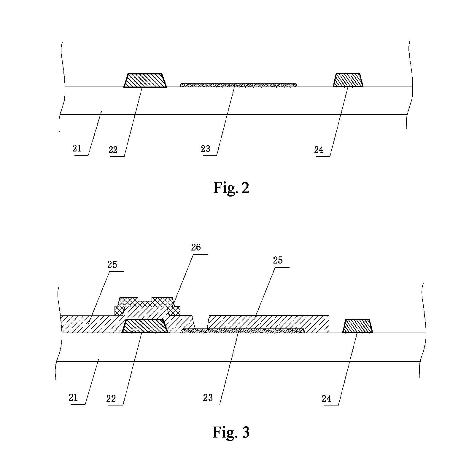
[0083]depositing the pixel electrode layer and the gate metallic layer on the glass substrate, predetermining thickness of the pixel electrode layer and thickness of the gate metallic layer, coating a first photoresist on the pixel electrode layer and the gate metallic layer, for examp...


PUM

PropertyMeasurementUnit
thicknessaaaaaaaaaa
metallicaaaaaaaaaa
sizeaaaaaaaaaa

Abstract

A method for manufacturing an array substrate for producing an amorphous silicon (a-Si) array substrate of a low-definition OLED display is provided. The method includes: patterning a gate metal and a pixel electrode on a glass substrate by using a first mask which is a first half tone mask; patterning a gate insulation layer and a semiconductor layer on the glass substrate with a second mask which is a second half tone mask; forming source / drain metallic layers and a channel with a third mask; and forming a bank layer with a fourth mask. The a-Si array substrates of low-definition OLED display panels undertake less manufacturing processes, which means that mask plates are used less and cost is reduced.

Description

CROSS REFERENCE TO RELATED APPLICATION[0001]The present application is based on, and claims priority from, Chinese application number 201410121807.0, filed Mar. 28, 2014, the disclosure of which is hereby incorporated by reference herein in its entirety.BACKGROUND OF THE INVENTION[0002]1. Field of the Invention[0003]The present invention relates to manufacturing technology of organic light-emitting diode (OLED) displays, and more especially, to a method for manufacturing array substrates for producing thin film transistor (TFT) array substrates of OLED displays.[0004]2. Description of the Prior Art[0005]Display technology has been developed fast for years. Flat displays have replaced bulky cathode ray tube (CRT) displays and become part of our daily lives. A commonly used flat display comprises a liquid crystal display (LCD) and an OLED display. The above-mentioned flat displays have merits of small size, low power consumption, and no radiation, so the flat displays are leaders in t...

Claims


Application Information

Patent Timeline
Patent Type & Authority Patents(United States)
IPC IPC(8): H01L21/00H01L27/32H01L51/56H01L21/84H01L27/12
CPCH01L27/1222H01L27/1218H01L27/1288H01L27/127H01L27/3246H01L51/56H01L2227/323H01L27/124H10K59/122H10K59/1201H10K71/00
Inventor XU, XIANGYANG
Owner TCL CHINA STAR OPTOELECTRONICS TECH CO LTD
Why Eureka
Try Eureka