Laminated inductor and array thereof

a technology of laminated inductor and array, which is applied in the direction of inductance, basic electric elements, coils, etc., can solve the problems of easy degradation of high frequency characteristics of laminated inductor, easy creation of communication problems, and inability to easily remove noise generated at high frequencies. , to achieve the effect of reducing stray capacitance, reducing noise generation, and high self-resonance frequency

Inactive Publication Date: 2016-05-10
SAMSUNG ELECTRO MECHANICS CO LTD
View PDF8 Cites 0 Cited by
  • Summary
  • Abstract
  • Description
  • Claims
  • Application Information

AI Technical Summary

Benefits of technology

[0016]An aspect of the present invention provides a laminated inductor capable of having a high self-resonance frequency and efficiently removing noise generated at a high frequency by decreasing stray capacitance.

Problems solved by technology

As a result, an environment in which communications problems easily occur has been created.
However, in the laminated inductor according to the related art, stray capacitance may be easily generated between printed circuit boards (PCBs) such that high frequency characteristics of the laminated inductor may be easily degraded, and noise generated at high frequencies may not be easily removed.
In addition, contact between the pair of terminal electrodes and the pair of external connection conductors, a solder bridge or the like, at the time of mounting the inductor may be generated, such that it may be difficult to miniaturize the laminated inductor.

Method used


Image

  • Laminated inductor and array thereof
  • Laminated inductor and array thereof
  • Laminated inductor and array thereof

Examples


modified example

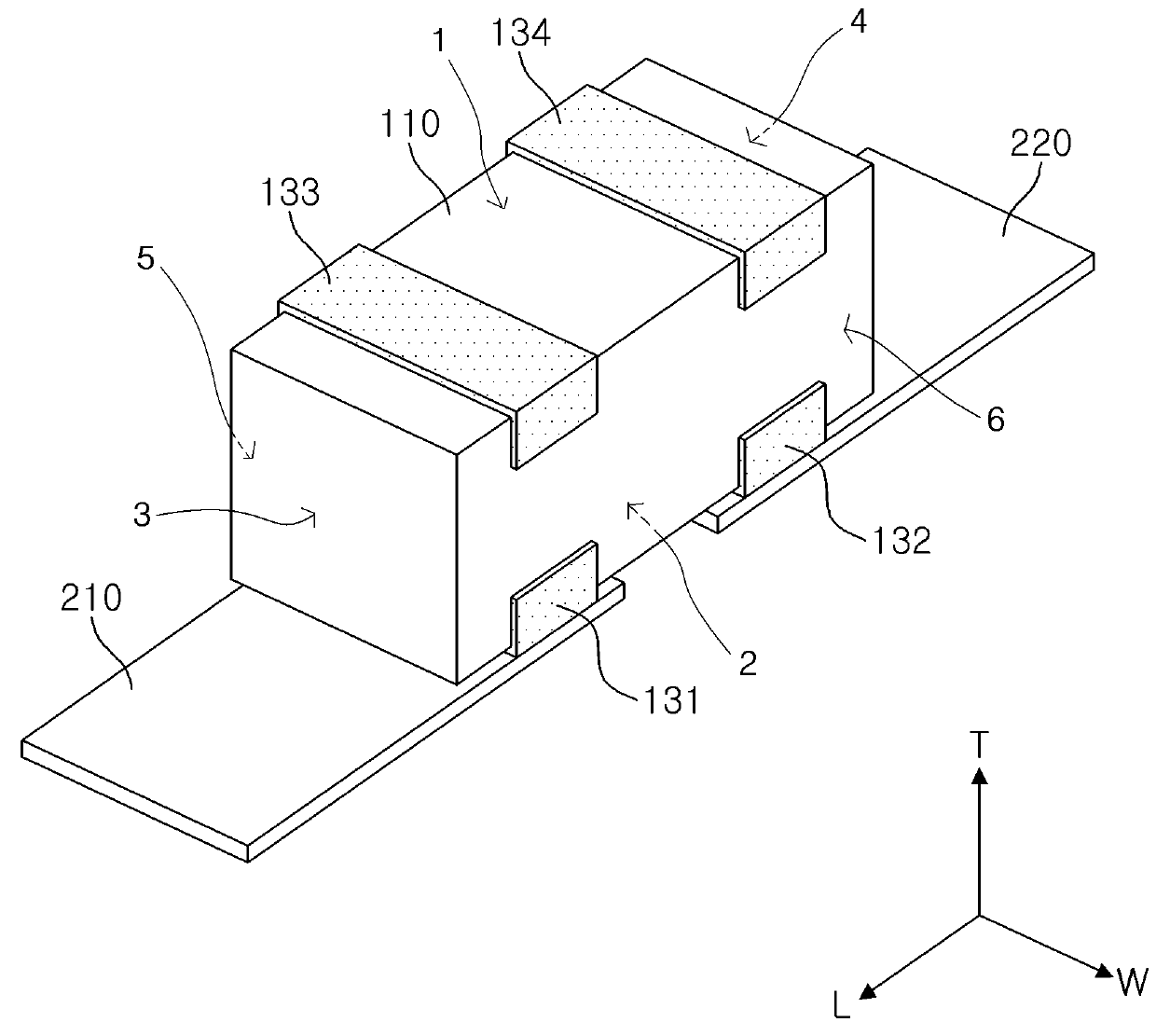
[0073]FIGS. 4 and 5 show a laminated inductor according to another embodiment of the invention.

[0074]Referring to FIGS. 4 and 5, a laminated inductor 100′ according to another embodiment of the invention has a first connection electrode 137 extended from the first main surface 1 of the body 110 to the third end surface 3 thereof, a first terminal electrode 135 extended from the second main surface 2 of the body 110 to the third end surface 3 thereof and spaced apart from the first connection electrode 135, a second connection electrode 138 spaced apart from the first connection electrode 137 of the body 110 and extended from the first main surface 1 of the body 110 to the fourth end surface 4 thereof, and a second terminal electrode 136 spaced apart from the first terminal electrode 135 and extended from the second main surface 2 of the body 110 to the fourth end surface 4 thereof.

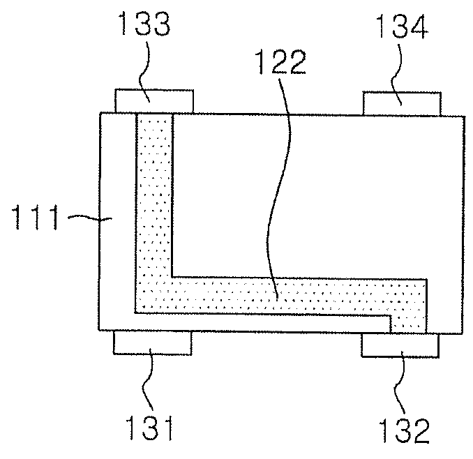
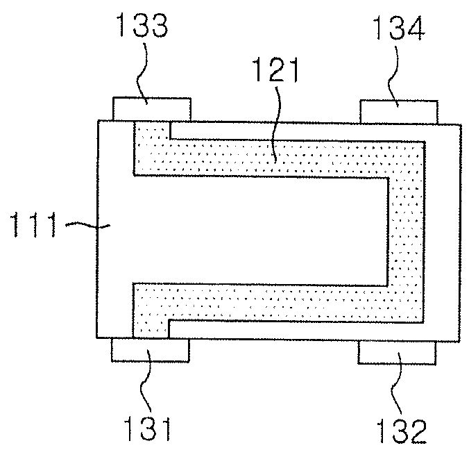
[0075]A first internal conductive pattern 124 may be configured to connect the first connection electro...


PUM

PropertyMeasurementUnit
thicknessaaaaaaaaaa
conductiveaaaaaaaaaa
internal conductiveaaaaaaaaaa

Abstract

There is provided a laminated inductor including: a body having a plurality of sheets laminated in a width direction, and having first and second main surfaces in a thickness direction, third and fourth end surfaces in a length direction, and fifth and sixth side surfaces in the width direction; a first connection electrode formed on the first main surface of the body; first and second terminal electrodes formed on the second main surface of the body to be spaced apart from one another; a plurality of first internal conductive patterns connecting the first connection electrode and the first terminal electrode; and at least one or more second internal conductive patterns connecting the first connection electrode and the second terminal electrode.

Description

CROSS-REFERENCE TO RELATED APPLICATIONS[0001]This application claims the priority of Korean Patent Application No. 10-2013-0027535 filed on Mar. 14, 2013, in the Korean Intellectual Property Office, the disclosure of which is incorporated herein by reference.BACKGROUND OF THE INVENTION[0002]1. Field of the Invention[0003]The present invention relates to a laminated inductor and an array thereof.[0004]2. Description of the Related Art[0005]Recently, as cloud computing infrastructure has been implemented and smartphones, tablet PCs, and the like have emerged, the market for small portable communications terminals has grown rapidly.[0006]Particularly, in the case of portable communications terminals, market competition, manifested in product multi-functionalization and miniaturization / thinness, is becoming fierce. In this situation, wireless communications circuits are required to be modularized, such that multi-band communications and reductions in wireless communication circuit volum...

Claims


Application Information

Patent Timeline
Patent Type & Authority Patents(United States)
IPC IPC(8): H01F5/00H01F27/28H01F27/29H01F17/00
CPCH01F27/29H01F17/0013H01F17/00H01F27/28
Inventor PARK, HEUNG KILPARK, MIN CHEOL
Owner SAMSUNG ELECTRO MECHANICS CO LTD
Why Eureka
Try Eureka