Radio frequency filter and semiconductor processing device

A radio frequency filter, radio frequency signal technology, applied in impedance network, electrical components, multi-terminal network and other directions, can solve the problems of self-resonant frequency reduction, radio frequency filter can not filter, radio frequency filter self-resonant frequency reduction and other problems, to achieve higher Effects of stability and improved applicability

Active Publication Date: 2015-07-01
BEIJING NAURA MICROELECTRONICS EQUIP CO LTD
View PDF6 Cites 2 Cited by
  • Summary
  • Abstract
  • Description
  • Claims
  • Application Information

AI Technical Summary

Problems solved by technology

Moreover, in practical applications, the radio frequency power source RF often outputs not only high-frequency power signals, but also low-frequency power signals, so as to generate plasma by means of high-frequency power signals (for example, 40MHz, 60MHz), and by means of low-frequency power signals (for example, , 20MHz) to control the energy of the plasma incident on the surface of the substrate. Therefore, the radio frequency filter 11 needs to filter two or more radio frequency signals with greatly different frequencies at the same time, but due to the characteristics of the air core inductor itself, increasing The inductance value of the large air-core inductor can filter low-frequency RF signals, but it will reduce the self-resonant frequency of the RF filter, which makes the RF filter unable to filter high-frequency RF signals; reduce the air-core inductance The inductance value of the RF filter can increase the self-resonant frequency of the RF filter, and the increase of the self-resonant frequency allows the RF filter to filter high-frequency RF signals, but due to the reduction of the inductance value of the air core inductor, it cannot be used for low-frequency RF signals. filtering
[0005] It can be seen from the above that the RF filter using air core inductors cannot simultaneously filter two or more RF signals with greatly different frequencies.

Method used


Image

  • Radio frequency filter and semiconductor processing device
  • Radio frequency filter and semiconductor processing device
  • Radio frequency filter and semiconductor processing device

Examples


Embodiment Construction

[0025] In order to enable those skilled in the art to better understand the technical solution of the present invention, the radio frequency filter and semiconductor processing equipment provided by the present invention will be described in detail below with reference to the accompanying drawings.

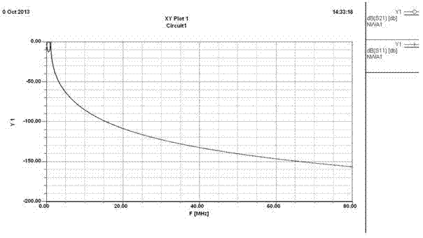
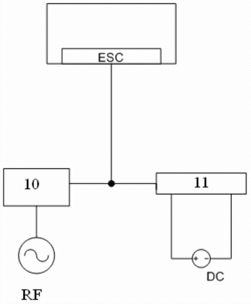
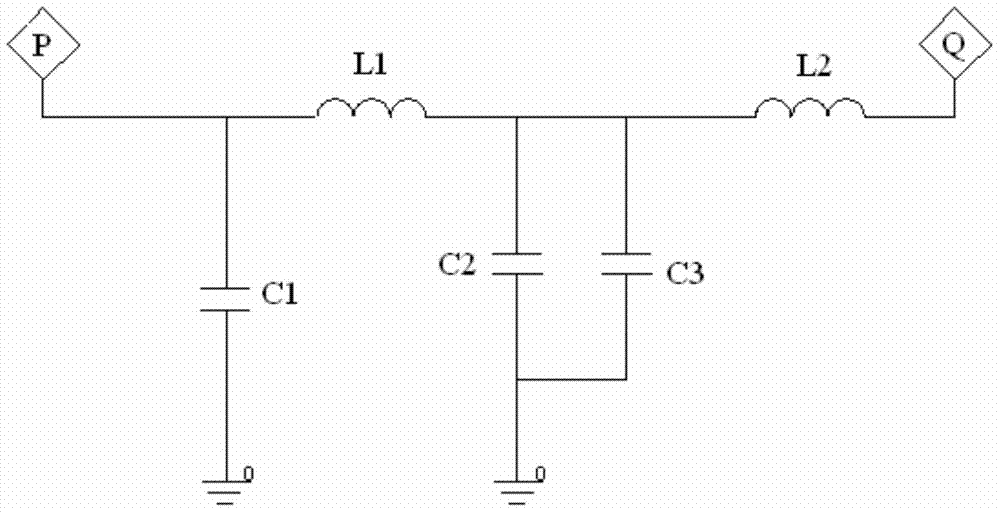
[0026] figure 2 A circuit diagram of a filter circuit of a radio frequency filter provided by an embodiment of the present invention. image 3 for figure 2 Schematic diagram of the structure of the inductance element in the filter circuit shown. Figure 4 It is a schematic diagram of connection of an ESC with a radio frequency filter provided by an embodiment of the present invention. Please also refer to figure 2 , image 3 and Figure 4 , the radio frequency filter 30 provided by the embodiment of the present invention is used to filter the radio frequency signal that flows back from the radio frequency power source RF connected to the electrostatic chuck ESC to the dire...


PUM


Abstract

The invention provides a radio frequency filter and a semiconductor processing device. The radio frequency filter is used for filtering radio frequency signals, which are returned by a radio frequency power source connected with an electrostatic chuck to a DC (direct current) power source connected with the electrostatic chuck. The radio frequency filter comprises an inductor element and a capacitor element, wherein the inductor element is a magnetic core inductor. The radio frequency filter can filter low-frequency radio frequency signals as well as high-frequency radio frequency signals simultaneously and accordingly can filter two or more radio frequency signals with large frequency differences, thereby enhancing the applicability.

Description

technical field [0001] The invention belongs to the technical field of semiconductor equipment manufacturing, and in particular relates to a radio frequency filter and semiconductor processing equipment. Background technique [0002] In the manufacturing process of semiconductor devices, an electrostatic chuck (ESC) is usually used to generate electrostatic attraction to attract the semiconductor wafer on it, so as to realize deposition, etching, etc. on the surface of the semiconductor wafer as the substrate. crafting process. [0003] Specifically, a lower electrode is provided in the ESC, and the lower electrode is electrically connected to a direct current power supply DC, and the direct current power supply DC is used to provide a certain direct current bias voltage to the lower electrode, so that the ESC generates electrostatic attraction to adsorb the substrate; and, because Processes such as deposition and etching on the surface of the substrate are carried out in a...

Claims


Application Information

Patent Timeline
Patent Type & Authority Applications(China)
IPC IPC(8): H03H7/00H03H3/02
Inventor 张超陈鹏师帅涛
Owner BEIJING NAURA MICROELECTRONICS EQUIP CO LTD
Why Eureka
Try Eureka