Ceramic electronic component

a technology of electronic components and ceramics, applied in the direction of capacitor details, electrical devices, capacitors, etc., can solve the problems of insufficient b>2/b>, insufficient b>8/b>, and the intrinsic function of the metal terminal, so as to reduce or prevent the generation of vibration sound, reduce or prevent the transmission of vibration, and hinder the elastic deformation of the metal terminal

Active Publication Date: 2016-05-31
MURATA MFG CO LTD
View PDF16 Cites 7 Cited by
  • Summary
  • Abstract
  • Description
  • Claims
  • Application Information

AI Technical Summary

Benefits of technology

[0011]Accordingly, preferred embodiments of the present invention provide a ceramic electronic component that significantly reduces or prevents generation of vibration sound due to vibration of a mounting substrate caused by a mechanical strain in an electronic component body of a ceramic electronic component.
[0016]According to a ceramic electronic component according to a preferred embodiment of the present invention, a plating-removal portion from which the plated film is removed is located on a peripheral surface of the mounting portion of the metal terminal, and thus a base material of the metal terminal is exposed. Accordingly, when mounting the ceramic electronic component to the mounting substrate with mounting solder, since wetting of the mounting solder to the metal terminal is significantly reduced or prevented, wetting of the mounting solder to a gap portion between the electronic component body and the metal terminal is significantly reduced or prevented, and thus it is possible to prevent the gap portion from being filled with the mounting solder. Accordingly, it is possible to sufficiently secure a space of the gap portion, and thus it is possible to significantly reduce or prevent transmission of vibration to the mounting substrate without hindering elastic deformation of the metal terminal. As a result, it is possible to significantly reduce or prevent generation of a vibration sound based on vibration of the mounting substrate due to a mechanical strain in the electronic component body of the ceramic electronic component.
[0017]In addition, in a case where the plating-removal portion is formed on a peripheral surface of the extension portion, it is possible to further suppress wetting of the mounting solder to the metal terminal, and thus it is possible to further suppress wetting of the mounting solder to the gap portion between the electronic component body and the metal terminal.
[0018]In addition, in a case where the plating-removal portion is provided on a peripheral surface of the terminal bonding portion, it is also possible to significantly reduce or prevent wetting of the mounting solder to the metal terminal, and thus it is possible to further reduce or prevent wetting of the mounting solder to the gap portion between the electronic component body and the metal terminal.
[0019]According to various preferred embodiments of the present invention, a ceramic electronic component, which contributes to significantly reducing or preventing generation of a vibration sound caused by vibration of a mounting substrate due to a mechanical strain in an electronic component body of a ceramic electronic component, is obtained.

Problems solved by technology

When vibration due to the strain is transmitted to the mounting substrate 7 through the outer electrodes 6, the entirety of the mounting substrate 7 serves as an acoustic radiation surface, and thus there is a concern that acoustic noise may be generated.
As a result, the intrinsic function of the metal terminal 8, which suppresses transmission of vibration of the stacked ceramic capacitor 2, may be insufficient in some cases.
As a result, vibration of the stacked ceramic capacitor 2 tends to propagate to the mounting substrate 7 through the pair of metal terminals 8, and thus acoustic noise due to substrate vibration tends to occur.

Method used


Image

  • Ceramic electronic component
  • Ceramic electronic component
  • Ceramic electronic component

Examples


Embodiment Construction

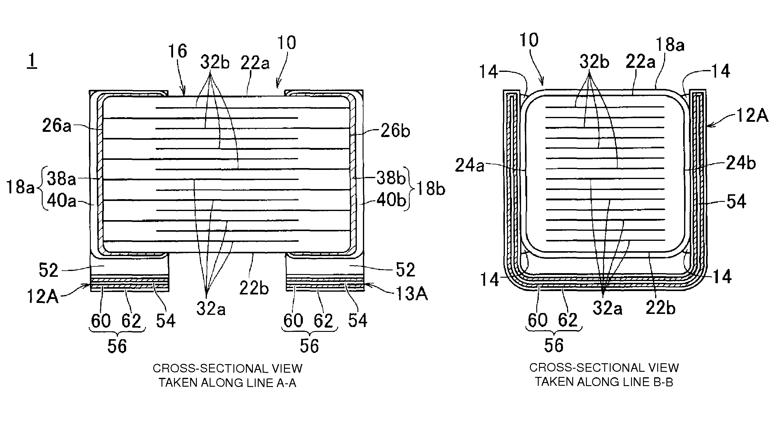
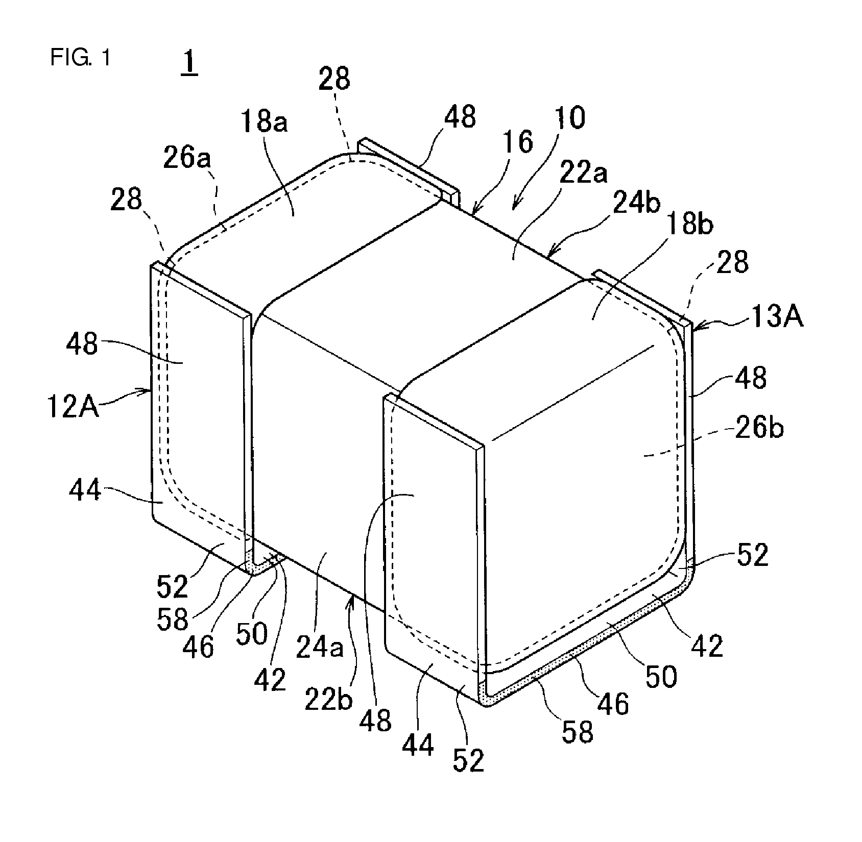
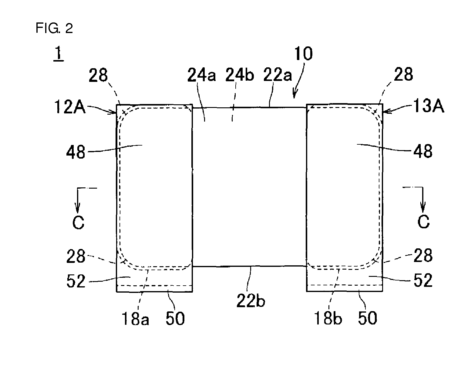
[0052]An example of a preferred embodiment of a ceramic electronic component according to the present invention will be described. FIG. 1 is an external perspective view illustrating an example of a ceramic electronic component according to a preferred embodiment of the present invention, FIG. 2 is a side view illustrating an example of the ceramic electronic component according to a preferred embodiment of the present invention, and FIG. 3 is a top view illustrating an example of the ceramic electronic component according to a preferred embodiment of the present invention. FIG. 4A is a cross-sectional view illustrating a cross-section taken along line A-A in FIG. 3, and FIG. 4B is a cross-sectional view illustrating a cross-section taken along line B-B in FIG. 3. FIG. 5 is a cross-sectional view illustrating a cross-section taken along line C-C in FIG. 2. FIG. 6 is an external perspective view of a metal terminal that is used in the ceramic electronic component according to a prefe...


PUM

PropertyMeasurementUnit
dielectric constantaaaaaaaaaa
relative dielectric constantaaaaaaaaaa
thicknessaaaaaaaaaa

Abstract

A ceramic electronic component includes an electronic component body and a pair of metal terminals. The electronic component body includes a ceramic element assembly and outer electrodes. The pair of metal terminals are connected to the outer electrodes by a bonding member. Each of the pair of metal terminals includes a terminal body and a plated film that is located on a surface of the terminal body. In addition, each of the pair of metal terminals includes a terminal bonding portion, a mounting portion, and an extension portion that is provided between the terminal bonding portions and the mounting portion. A plating-removal portion from which the plated film is removed is provided at least at a peripheral surface of the mounting portion, and thus a surface of the terminal body is exposed.

Description

BACKGROUND OF THE PRESENT INVENTION[0001]1. Field of the present invention[0002]The present invention relates to a ceramic electronic component which includes a stacked ceramic capacitor.[0003]2. Description of the Related Art[0004]In recent years, reduction in size and increase in functionality of electronic apparatuses have rapidly progressed. Reduction in size of a stacked ceramic capacitor that is mounted on an electronic apparatus has also been desired. For example, a stacked ceramic capacitor having a large electrostatic capacity is commercially produced as an alternative to an aluminum electrolytic capacitor due to the progress of a thin-layer technique and a multi-layer technique.[0005]As illustrated in FIG. 26, a stacked ceramic capacitor 2 that is an electronic component body includes a ceramic element assembly 5 in which a plurality of ceramic layers 3 and a plurality of inner electrodes 4 are alternately stacked. Adjacent inner electrodes of the plurality of inner electr...

Claims


Application Information

Patent Timeline
Patent Type & Authority Patents(United States)
IPC IPC(8): H01G4/30H01G2/06H01G4/232H01G4/228
CPCH01G2/065H01G4/232H01G4/30H01G4/2325
Inventor ITAGAKI, YOJI
Owner MURATA MFG CO LTD
Why Eureka
Try Eureka