Switch module
a switch module and switch technology, applied in the direction of cross-talk/noise/interference reduction, printed circuit grounding, printed circuit non-printed electric components association, etc., can solve the problem of front-end circuit fec characteristics degradation, and achieve the effect of preventing the generation of undeired coupling within the common-terminal-side circuit and significantly reducing or preventing the degradation of switch module characteristics
- Summary
- Abstract
- Description
- Claims
- Application Information
AI Technical Summary
Benefits of technology
Problems solved by technology
Method used
Image
Examples
first preferred embodiment
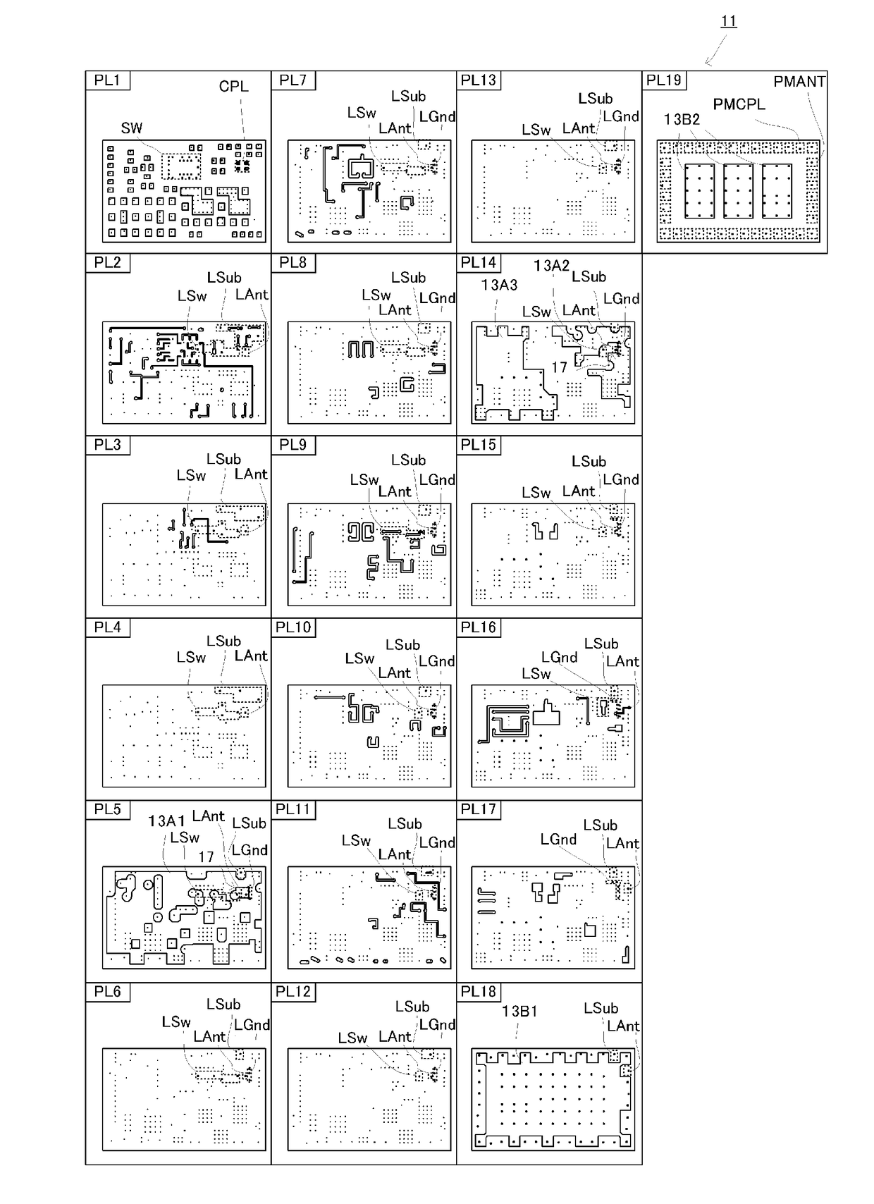
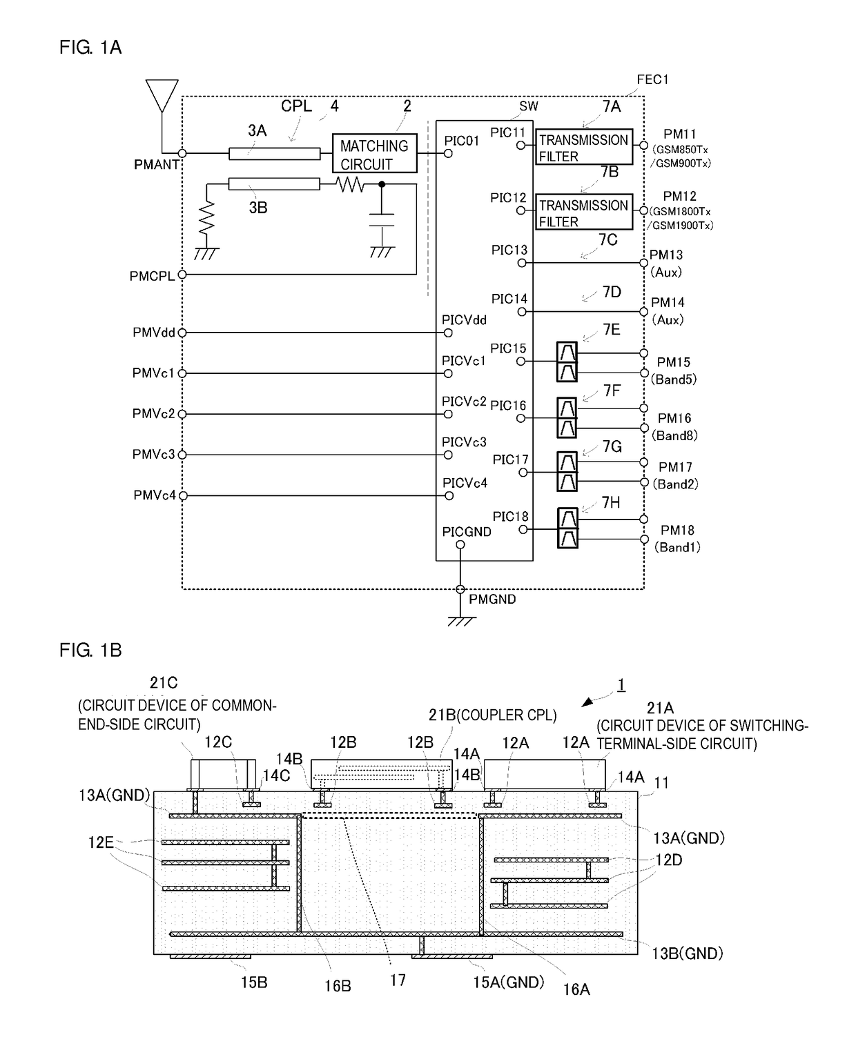
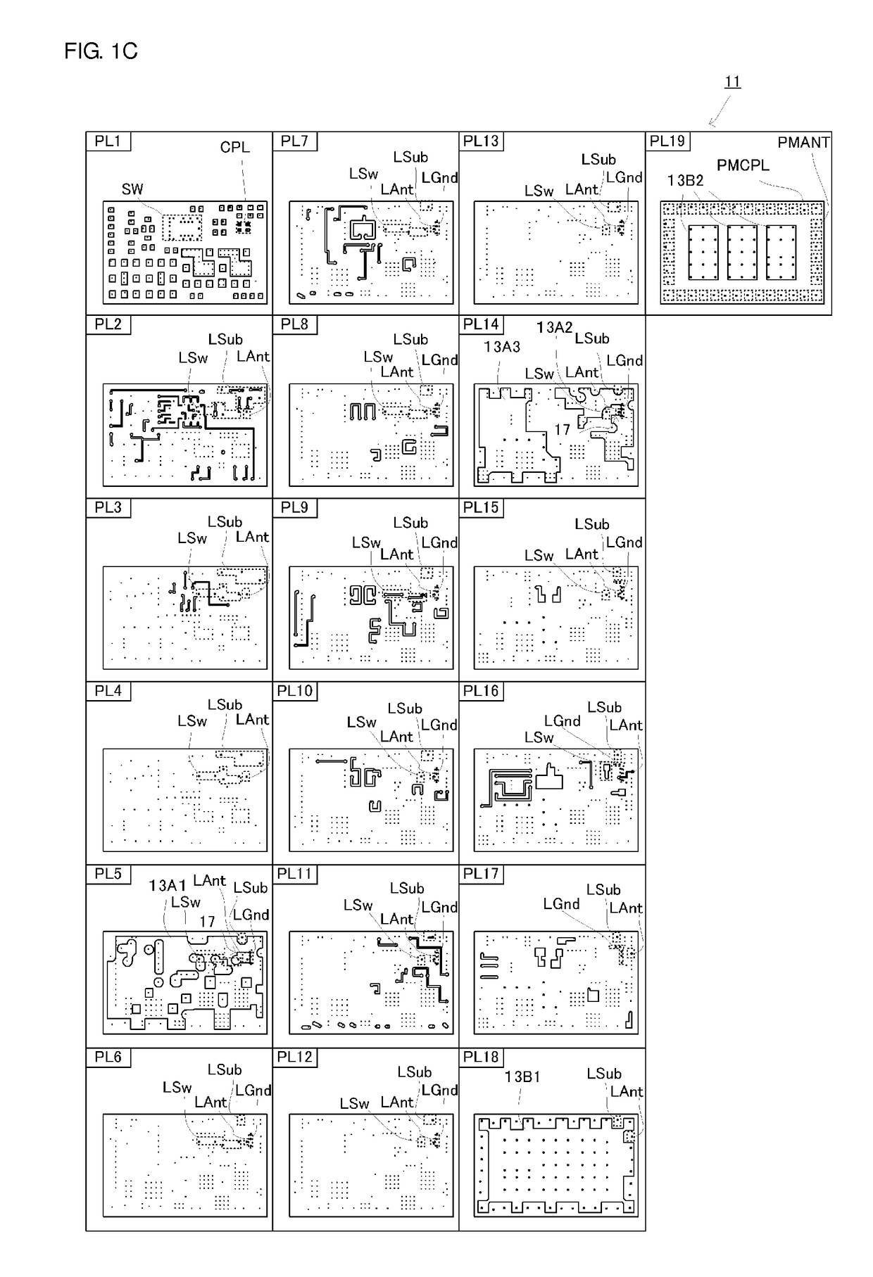
[0038]Hereinafter, a switch module according to a first preferred embodiment of the present invention will be described with reference to FIG. 1A to FIG. 1D.
[0039]FIG. 1A is a block diagram illustrating the circuit configuration of a first preferred embodiment of the present invention. A front-end circuit FEC1 illustrated in FIG. 1A includes a switch circuit SW, a common-terminal-side circuit 4, and switching-terminal-side circuits 7A to 7H.
[0040]The switch circuit SW includes a power supply port PICVdd, control ports PICVc1 to PICVc4, a common port PIC01, and switching ports PIC11 to PIC18. The power supply port PICVdd is a port to which a driving voltage of the switch circuit SW is applied. The control ports PICVc1-PICVc4 are ports to which respective control voltages are applied. The common port PIC01 is a port corresponding to the common terminal in the present preferred embodiment. The switching ports PIC11 to PIC18 are ports corresponding to the switching terminals in the pres...
second preferred embodiment
[0083]Hereinafter, a switch module according to a second preferred embodiment of the present invention will be described with reference to FIG. 2A and FIG. 2B.
[0084]FIG. 2A is a block diagram illustrating the circuit configuration of a switching module according to the present preferred embodiment. A front-end circuit FEC2 illustrated in FIG. 2A includes a switch circuit SW, a common-terminal-side circuit 4, and switching-terminal-side circuits 7A to 7H. Note that the internal configurations of the switch circuit SW, the common-terminal-side circuit 4, and the switching-terminal-side circuits 7A and 7B are preferably the same as those of the front-end circuit FEC1 according to the first preferred embodiment and, hence, the descriptions thereof are omitted here. The front-end circuit FEC2 has a configuration in which the duplexers have been removed from the front-end circuit FEC1 of the first preferred embodiment and the switching-terminal-side circuits 7C to 7H include transmission ...
third preferred embodiment
[0106]Hereinafter, a switch module according to a third preferred embodiment of the present invention will be described with reference to FIG. 3. Note that a block diagram illustrating the circuit configuration of the switch module according to the present preferred embodiment is preferably the same as that of the front-end circuit FEC1 and, hence, description thereof is omitted here. Further, the schematic diagram of the cross-sectional configuration of the switch module according to the present preferred embodiment is preferably the same as that of the switch module 1 according to the first preferred embodiment and, hence, description thereof is omitted here.
[0107]FIG. 3 is a stacking diagram illustrating a multilayer substrate 31 of an example of the switch module according to the third preferred embodiment of the present invention. The multilayer substrate 31 illustrated here preferably includes 19 layers of ceramic layers (dielectric layers) stacked on top of one another. In th...
PUM
 Abstract
Description
Claims
Application Information


