
Variable-size solder bump structures for integrated circuit packaging
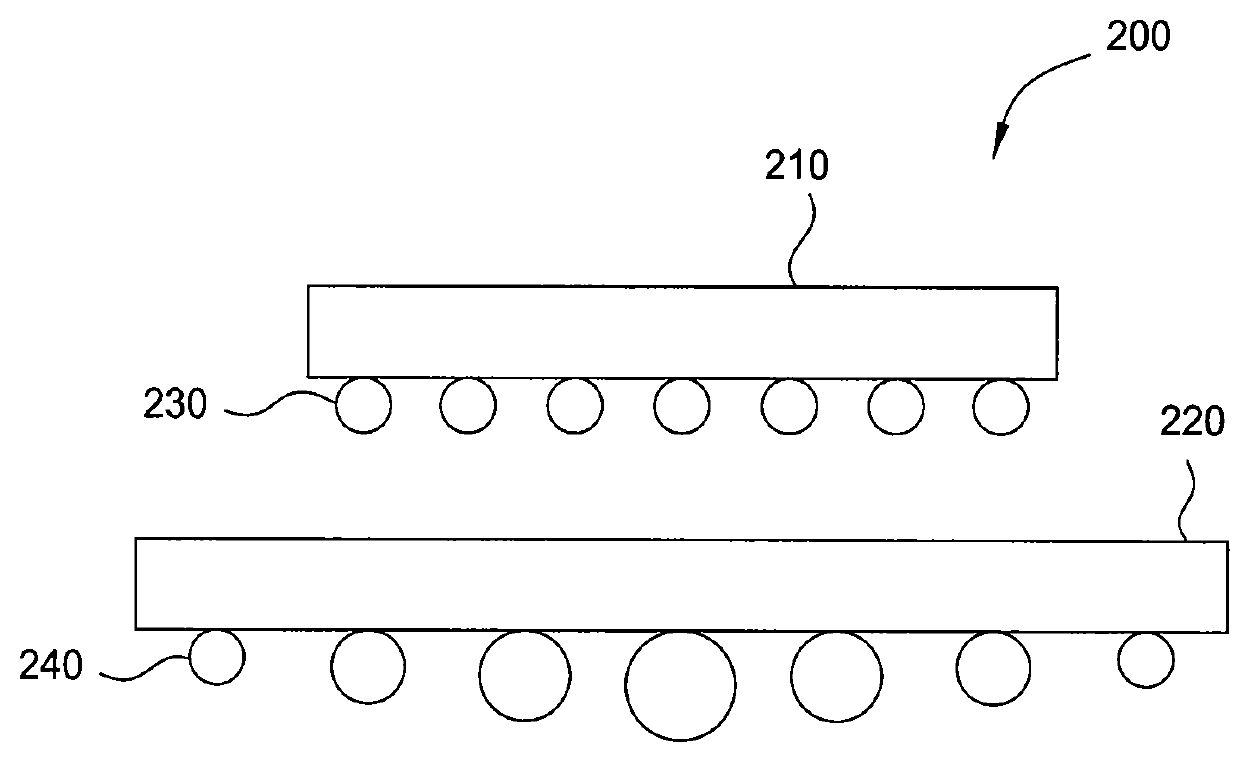
a technology of integrated circuit packaging and solder bumps, which is applied in the direction of printed circuit manufacturing, printed circuit aspects, and testing/measurement of semiconductor/solid-state devices, etc., can solve the problems of reducing the planarity warping and affecting the electrical connection provided, so as to improve the yield of the ic package
- Summary
- Abstract
- Description
- Claims
- Application Information
AI Technical Summary
Benefits of technology
Problems solved by technology
Method used
Image

Examples
Embodiment Construction
[0018]In the following description, numerous specific details are set forth to provide a more thorough understanding of embodiments of the present invention. However, it will be apparent to one of skill in the art that embodiments of the present invention may be practiced without one or more of these specific details.
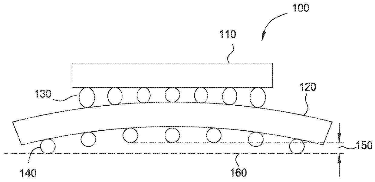
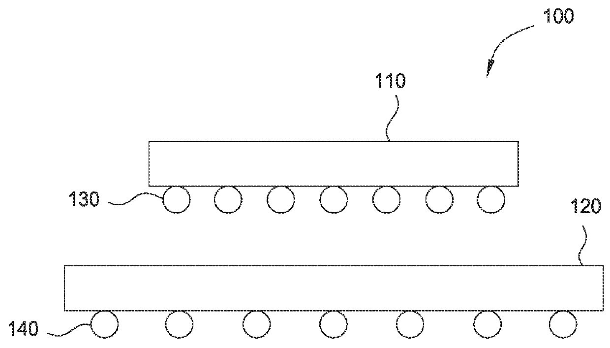
[0019]FIGS. 1A and 1B illustrate schematic views of an integrated circuit (IC) package 100 having a conventional configuration. The conventional IC package 100 includes a die 110, a substrate 120, a first plurality of solder balls 130, and a second plurality of solder balls 140. The first plurality of solder balls 130 mechanically and electrically couple the die 110 to the substrate 120 and provide electrical connections between the die 110 and the substrate 120. The second plurality of solder balls 140 mechanically and electrically couple the conventional IC package 100 to a circuit board (not shown) and provide electrical connections between the conventional IC packag...
PUM
 Abstract
Description
Claims
Application Information