Staggered wirebonding configuration

a wirebonding configuration and finger technology, applied in the direction of electrical equipment, semiconductor devices, semiconductor/solid-state device details, etc., can solve the problem of confined pitch of the bonding pad, achieve the effect of reducing the cost of the chip package, increasing the number of bonding pads, and enhancing chip efficiency

Active Publication Date: 2008-08-12
ADVANCED SEMICON ENG INC
View PDF8 Cites 10 Cited by
  • Summary
  • Abstract
  • Description
  • Claims
  • Application Information

AI Technical Summary

Benefits of technology

[0011]An object of the invention is to provide a staggered finger configuration and a semiconductor chip package applicable to chips with different arrangements of staggered bonding pads, in order to reduce the cost from additional design of fingers on a substrate, and forming more bonding pads to enhance the chip efficiency.
[0015]In addition, the staggered bonding pads can replace the conventional single in-line bonding pads to increase the number of the bonding pads on a chip, thereby enhancing the chip efficiency, reducing the cost of the package for chips and improving the package yield for chips.

Problems solved by technology

Nevertheless, the pitch of the bonding pads is confined by the design rule of wire bonding process, remaining unable to scale down to match the conductive wires.

Method used


Image

  • Staggered wirebonding configuration
  • Staggered wirebonding configuration
  • Staggered wirebonding configuration

Examples


Embodiment Construction

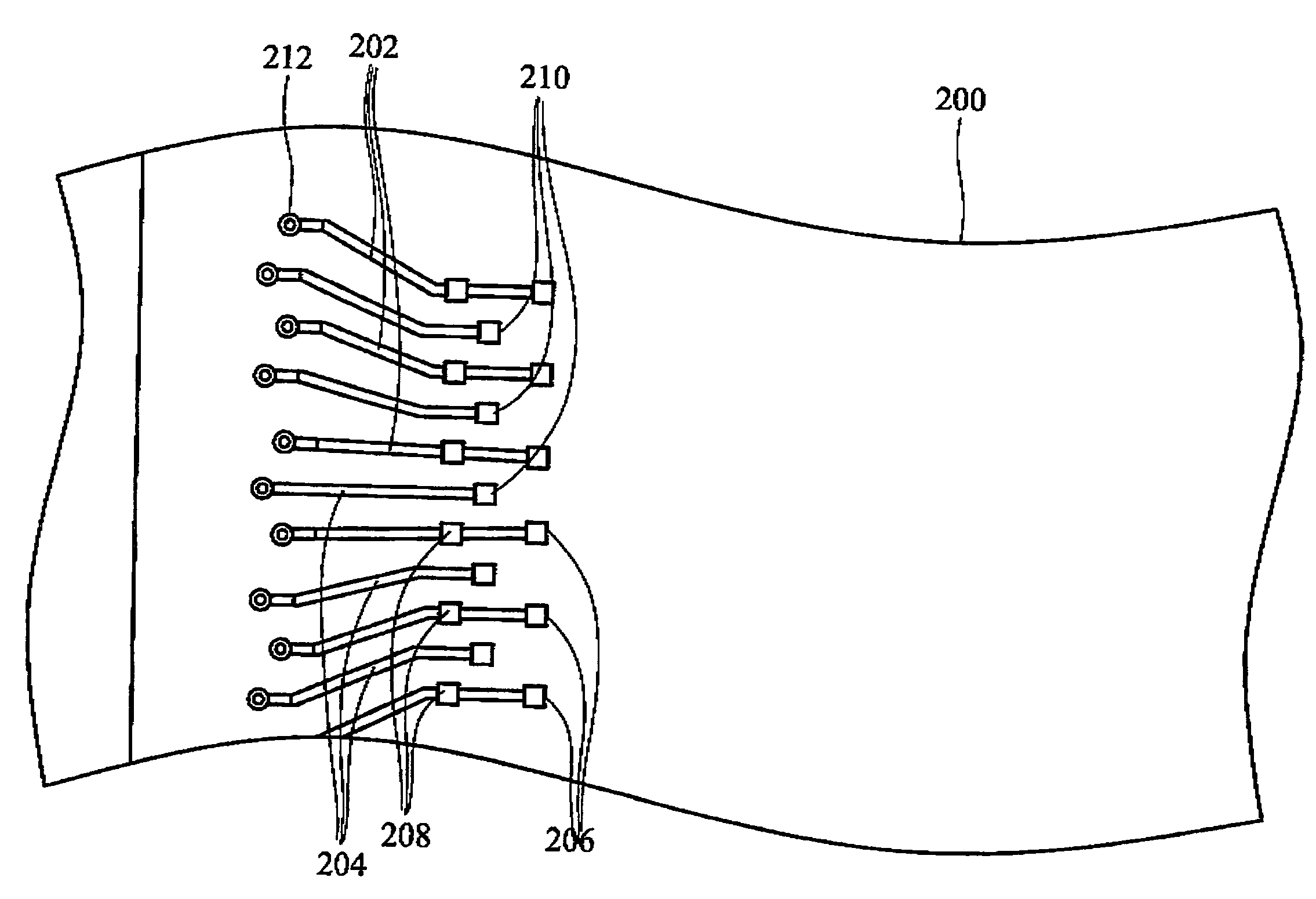
[0025]FIG. 4 is a top view of a substrate bearing a staggered finger configuration according to an embodiment of the invention. In this embodiment, a substrate 200 has a plurality of first and second conductive wires arranged alternately thereon. Each of the first conductive wires connects to a pair of inner and an outer finger 206, 208, and each of the second conductive wires connects to an intermediate finger between the inner and outer fingers 206, 208, providing a staggered finger configuration connecting to signal pads on the chip. The substrate 200 may be a core substrate with vias, blind vias or buried vias. Additionally, the substrate 200 and the first and the second conductive wires 202, 204 further comprise a solder mask 24030 thereon (as shown in FIG. 7). The fingers 206, 208, and 210 are exposed under openings of the solder mask 240. In this embodiment, the openings may be rectangular or other shape such as square, circular or polygonal.

[0026]Again referring to FIG. 4, t...


PUM


Abstract

The present invention discloses a staggered finger configuration comprising a plurality of first and second conducting wires alternately arranged on the substrate, wherein each of the first conducting wire connecting an inner and an outer fingers and each of the second conducting wire connecting an intermediate finger between the inner and the outer fingers, thereby forming a staggered configuration.

Description

[0001]This application claims foreign priority under 35 USC 119 of Taiwan Application Serial No. 093133828, filed May 11, 2004, which is hereby incorporated by reference.BACKGROUND[0002]The present invention relates in general to a staggered finger configuration and more particularly to a staggered finger configuration for chips with staggered bonding pads.[0003]As the efficiency and complexity of semiconductor chips increase, semiconductor packages provide increased efficiency.[0004]In wire bonding, the arrangement of bonding pads on a chip is important. In a package process such as ball grid array (BGA), the pitch of conductive wires on a substrate can be very small due to photolithography technique. Nevertheless, the pitch of the bonding pads is confined by the design rule of wire bonding process, remaining unable to scale down to match the conductive wires. As a result, the arrangement of bonding pads has become a critical parameter in package efficiency.[0005]Generally, the num...

Claims


Application Information

Patent Timeline
Patent Type & Authority Patents(United States)
IPC IPC(8): H01L23/48H01L21/56H01L21/607H01L23/04H01L23/485H01L23/498
CPCH01L21/565H01L23/49838H01L24/06H01L24/49H01L24/85H01L2224/05553H01L2224/05599H01L2224/45111H01L2224/45116H01L2224/45147H01L2224/45155H01L2224/48091H01L2224/48095H01L2224/48227H01L2224/48228H01L2224/49109H01L2224/49171H01L2224/49431H01L2224/49433H01L2224/73265H01L2224/85399H01L2924/01022H01L2924/01028H01L2924/01029H01L2924/01046H01L2924/01047H01L2924/0105H01L2924/01057H01L2924/01079H01L2924/01082H01L2924/014H01L24/48H01L2924/00014H01L2924/01024H01L2924/01033H01L2224/32225H01L2224/48799H01L2224/05554H01L2224/78H01L2924/00H01L2224/45099H01L2924/00012H01L24/73H01L2924/181
Inventor DING, YI-CHUAN
Owner ADVANCED SEMICON ENG INC
Why Eureka
Try Eureka