Method and structure for prevention leakage of substrate strip

a substrate strip and leakage prevention technology, applied in the direction of resist details, non-metallic protective coating application, circuit inspection/indentification, etc., can solve the problems of increasing packaging procedure and cost, affecting the package structure and reliability of the package substrate, and damaging the electrical functions of the chips on the substrate strip

Inactive Publication Date: 2006-08-15
ADVANCED SEMICON ENG INC
View PDF2 Cites 10 Cited by
  • Summary
  • Abstract
  • Description
  • Claims
  • Application Information

AI Technical Summary

Benefits of technology

[0005]A main purpose of the present invention is to supply a method for manufacturing a substrate strip. The substrate strip includes at least one plating bus at the edge portion and a plurality of plating lines at the units. The plating bus has an extended trail extended to the sidewall of the substrate strip. After formation of a solder mask on the substrate strip and formation of a surface layer on the contact pads, a breaking hole is formed at the edge portion so that the extended trail is electrically isolated from the contact pads in order to prevent a chip on the substrate strip from being damaged by ESD while conveying during packaging processes, and to increase packaging yield without extra hole-drilling processes in units.
[0006]According to the present invention, a substrate strip is provided comprising an edge portion and a plurality of units. The substrate strip has a surface and a sidewall. A patterned metal layer is formed on the surface of the substrate strip. The patterned metal layer includes at least one plating bus extended to the edge portion, a plurality of plating lines at the units, a plurality of contact pads at the units and a plurality of fiducial marks at the edge portion. The contact pads are electrically connected to the plating bus via the plating lines. The plating bus has an extended trail having one end exposed out of the sidewall of the substrate strip. A solder mask is formed on the surface of the substrate strip. The solder mask has a plurality of first openings exposing the contact pads and the fiducial marks, and at least a second opening at the edge portion exposing a predetermined portion of the plating bus, if necessary. Thereafter, a surface layer is formed on the contact pads and the fiducial marks. After removing the exposed portion of the plating bus by etching, mechanical drilling or laser drilling, a breaking hole is formed to electrically isolate the extended trail of the plating bus from the contact pads. Leakage between a chip on the substrate strip and the plating bus is avoided, the chip cannot be damaged by ESD during packaging process in a simple formation of the breaking hole.

Problems solved by technology

The ESD (Electrostatic Discharge) will occur by the contact between the exposed plating buses at the sidewalls of the package substrate strip and the conveying track, which will damage the electrical functions of chips on the substrate strip.
Nevertheless, the drilling holes are formed at the units, they may affect the package structure and reliability of the package substrates.
To avoid this, they have to be filled with an insulation material, and this would increase packaging procedure and cost.

Method used


Image

  • Method and structure for prevention leakage of substrate strip
  • Method and structure for prevention leakage of substrate strip
  • Method and structure for prevention leakage of substrate strip

Examples


first embodiment

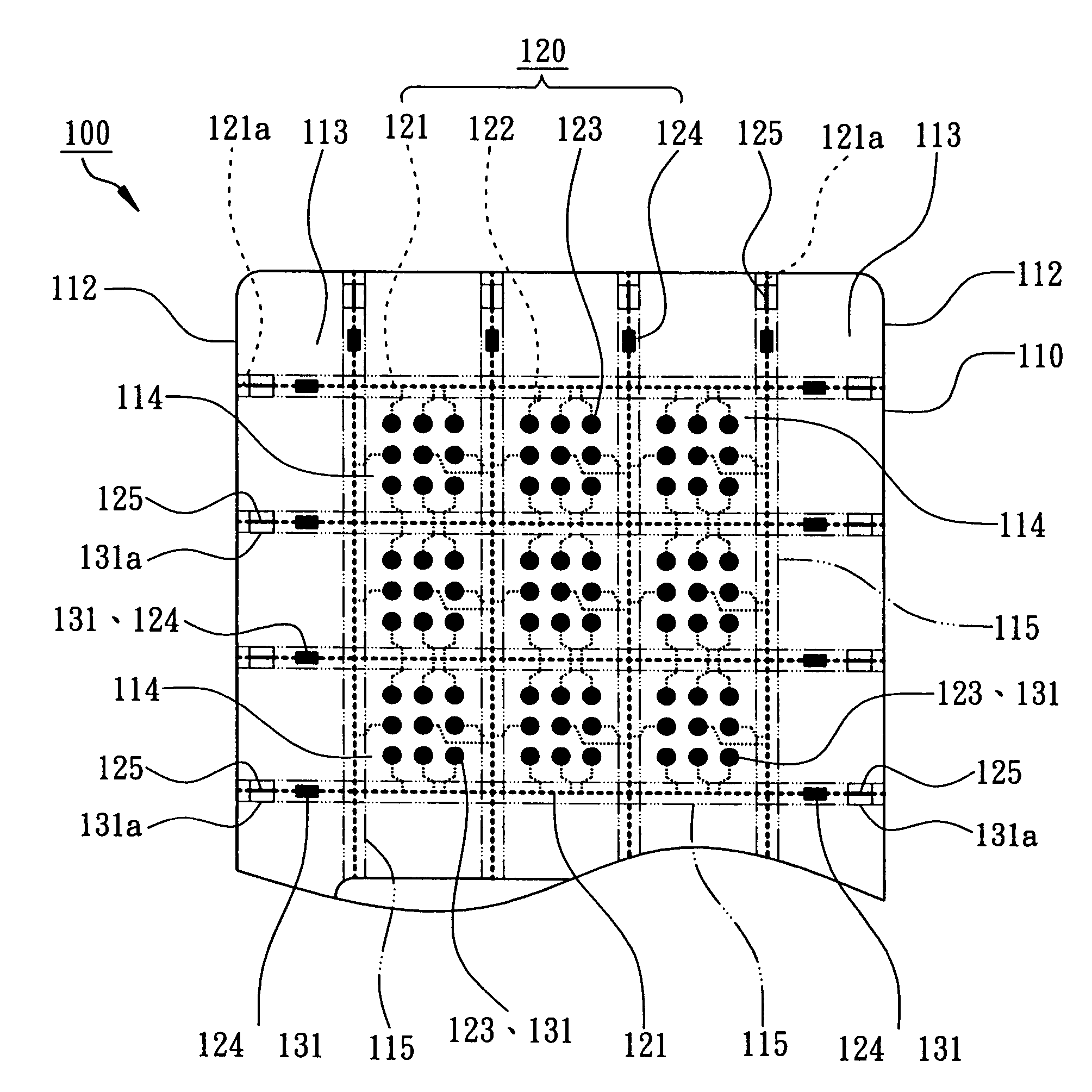
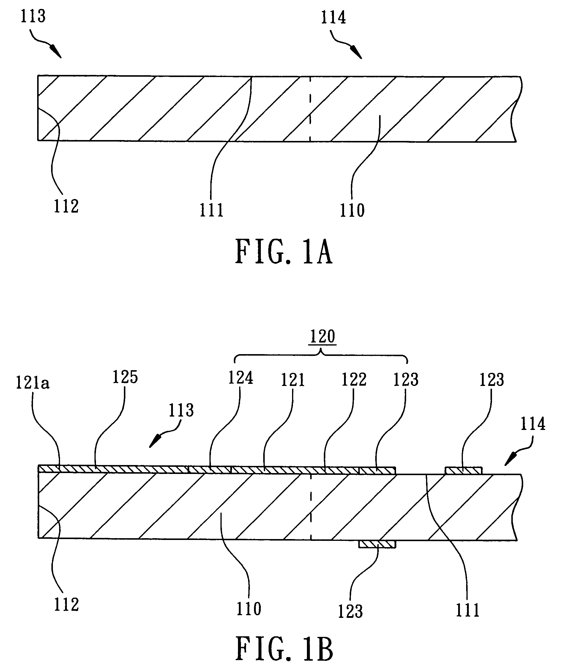
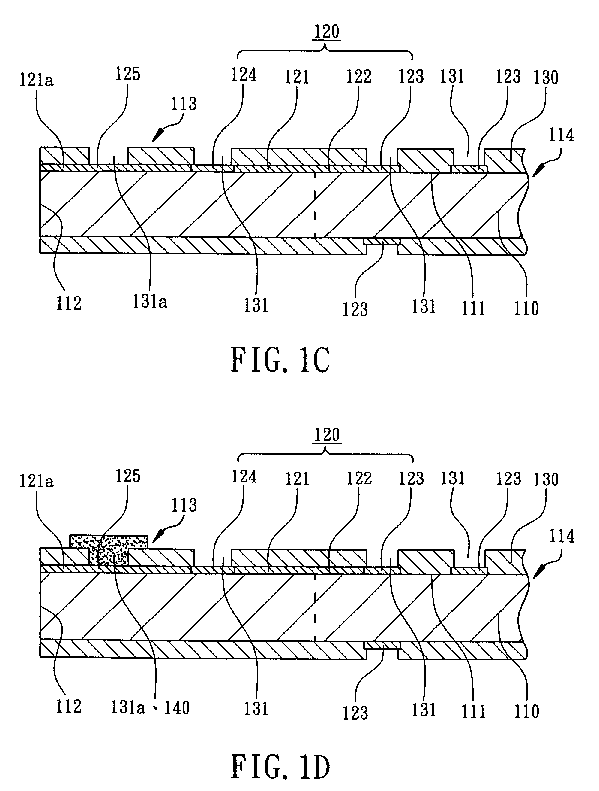
[0012]According to the present invention, a method for manufacturing a substrate strip body 110 is disclosed. As shown in FIGS. 1A and 2, a substrate strip 110 is provided. The substrate strip 110 has a surface 111 and at least one sidewall 112, and the substrate strip 110 also includes at least one edge portion 113 and a plurality of units 114. The units 114 are arranged in at least one matrix and are surrounded by the edge portion 113. Referring to FIG. 2, a plurality of scribe lines 115 are formed between the units 114 and extending to the edge portion 113.

[0013]As shown in FIGS. 1B and 2, a patterned metal layer 120 is formed on the surface 111 of the substrate strip 110. One of the methods to form the patterned metal layer 120 is to laminate a Cu foil on the surface 111 of substrate strip 110, and then patterned the Cu foil by exposure, development, and etching. The patterned metal layer 120 includes at least one plating bus 121 extended to the edge portion 113, a plurality of ...

second embodiment

[0019]According to the present invention, a method for manufacturing a package substrate strip is illustrated from FIG. 4A to 4E. Firstly as shown in FIG. 4A, a substrate strip 210 is provided. The substrate strip 210 has a surface 211 and a plurality of sidewalls 212. As shown in FIG. 4B, a patterned metal layer 220 is formed on the surface 211 of the substrate strip 210. The patterned metal layer 220 includes at least one plating bus 221 extended to an edge portion of the substrate strip 210, a plurality of plating lines 222 in units of the substrate strip 210, a plurality of contact pads 223 in units of the substrate strip 210, a plurality of fiducial marks 224 at the edge portion of the substrate strip 210. The plating bus 221 defines at least a pre-cut point 225 and is electrically connected to the contact pads 223 via the plating lines 222. The plating bus 221 has an extended trails 221a having one end exposed out of one of the sidewalls 212. The fiducial marks 224 are also fo...


PUM


Abstract

The present invention provides a structure and a method for prevention leakage of a substrate strip. The substrate strip includes an edge portion and a plurality of units. A patterned metal layer on a surface of the substrate strip includes at least one plating bus extended to the edge portion, a plurality of plating lines at the units, a plurality of contact pads at the units and a plurality of fiducial marks at the edge portion. The plating bus has an extended trail having one end exposed out of the sidewall of the substrate strip. The fiducial marks and the contact pads are exposed out of a plurality of first openings of a solder mask. The solder mask also has a second opening at the edge portion exposing a portion of the plating bus to define a breaking hole. After forming a surface layer on the fiducial marks and the contact pads, the exposed portion of the plating bus is void of the surface layer. By removing the exposed portion of the plating bus, the breaking hole is formed to electrically isolate the extended trail from the contact pads in order to prevent a chip on the substrate strip from being damaged by ESD (Electrostatic Discharge) during packaging processes.

Description

FIELD OF THE INVENTION[0001]The present invention relates to a package substrate strip and, more particularly, to a method and a structure for prevention leakage from plating buses.BACKGROUND OF THE INVENTION[0002]A conventional substrate strip for semiconductor packages is formed with plating buses and plating lines for plating a metal surface layer on contact pads. Normally the plating buses are extended to the sidewalls of the substrate strip. In the packaging processes, the substrate strip is conveyed by a track. The ESD (Electrostatic Discharge) will occur by the contact between the exposed plating buses at the sidewalls of the package substrate strip and the conveying track, which will damage the electrical functions of chips on the substrate strip. In order to prevent chips on the substrate strip from being damaged by ESD, R.O.C. Taiwan Pat. No. 508,769 discloses a conventional substrate strip with a layer of copper-mesh layer being electrically connected to the molding gate....

Claims


Application Information

Patent Timeline
Patent Type & Authority Patents(United States)
IPC IPC(8): H01L23/02H01L23/495H01L23/498H01L23/538H01L23/544H01L23/60H05K1/02H05K3/00H05K3/06H05K3/24H05K3/28
CPCH01L23/544H01L23/60H01L24/97H05K3/242H01L23/49838H01L2924/01033H01L2223/54473H01L2924/01029H01L2924/01078H01L2924/01079H05K1/0269H05K3/0047H05K3/0052H05K3/06H05K3/28H05K2201/09918H05K2203/0574H05K2203/175H01L2924/01006H01L23/5386H01L2924/12042H01L2924/00
Inventor CHEN, YING-CHIHTIEN, YUN-HSIANGLAI, MING-JIUNDING, YI-CHUAN
Owner ADVANCED SEMICON ENG INC
Why Eureka
Try Eureka